Visible to Intel only — GUID: aeg1659983971506
Ixiasoft
Visible to Intel only — GUID: aeg1659983971506
Ixiasoft
1.2.2. Functional Description for the Single Root I/O Virtualization (SR-IOV) Design Example
The SR-IOV design example performs memory transfers from a host processor to a target device. It only supports two Physical Functions (PFs) and 32 Virtual Functions (VFs) per PF. Note that this design example does not support back-to-back transactions from the host processor since the design is intended to showcase single-dword transactions. In addition, the addresses for all the transactions must be dword-aligned.
This design example automatically creates the files necessary to simulate and compile in the Quartus® Prime software. You can download the compiled design to an Agilex™ 7 I-Series FPGA Development Kit.
| Port Mode | Link Width | Link Speed | Data Width (Bits) | Design Example Support | Simulators Support |
|---|---|---|---|---|---|
| Endpoint | x16 | Gen 5 | 1024 (4 x 256) | SCTH | VCS* , VCS* MX, Siemens* EDA QuestaSim* , Xcelium* 4 |
| N/A | N/A | N/A | N/A | ||
| N/A | N/A | N/A | |||
| N/A | N/A | N/A | N/A | ||
| N/A | N/A | N/A | |||
| x8 | N/A | N/A | N/A | N/A | |
| N/A | N/A | N/A | N/A | ||
| N/A | N/A | N/A | |||
| N/A | N/A | N/A | N/A | ||
| N/A | N/A | N/A | |||
| x4 | N/A | N/A | N/A | N/A | |
| N/A | N/A | N/A | N/A | ||
| N/A | N/A | N/A | |||
| N/A | N/A | N/A | N/A | ||
| N/A | N/A | N/A | |||
| Root Port | N/A | N/A | N/A | N/A | N/A |
| TL Bypass | N/A | N/A | N/A | N/A | N/A |
| PIPE-D | N/A | N/A | N/A | N/A | N/A |
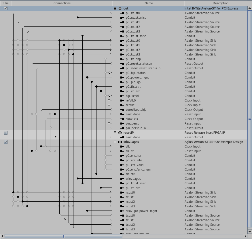
- The generated R-Tile Avalon Streaming (Avalon-ST) IP Endpoint variant (DUT) with the parameters you specified. This component drives the received TLP data to the SR-IOV application.
- The SR-IOV Application (APPS) component, which performs the necessary translation between the PCI Express TLPs and Avalon-ST writes and reads to the on-chip memory. For the SR-IOV APPS component, a memory read TLP generates a Completion with data.
- A Reset Release IP.
The simulation testbench instantiates the SR-IOV design example and a Root Port BFM to interface with the target Endpoint.
The test program writes to and reads back data from the same location in the on-chip memory across 2 PFs and 32 VFs per PF. It compares the data read to the expected result. The test reports, "Simulation stopped due to successful completion" if no errors occur.
