Visible to Intel only — GUID: wgz1526952909368
Ixiasoft
2.3.2.1. Using Simulation Signal Activity Data in Power Analysis
2.3.2.2. Signal Activities from RTL (Functional) Simulation, Supplemented by Vectorless Estimation
2.3.2.3. Signal Activities from Vectorless Estimation and User-Supplied Input Pin Activities
2.3.2.4. Signal Activities from User Defaults Only
2.5.1. Complete Design Simulation Power Analysis Flow
2.5.2. Modular Design Simulation Power Analysis Flow
2.5.3. Multiple Simulation Power Analysis Flow
2.5.4. Overlapping Simulation Power Analysis Flow
2.5.5. Partial Design Simulation Power Analysis Flow
2.5.6. Vectorless Estimation Power Analysis Flow
3.4.1. Clock Power Management
3.4.2. Pipelining and Retiming
3.4.3. Architectural Optimization
3.4.4. I/O Power Guidelines
3.4.5. Dynamically Controlled On-Chip Terminations (OCT)
3.4.6. Memory Optimization (M20K/MLAB)
3.4.7. DDR Memory Controller Settings
3.4.8. DSP Implementation
3.4.9. Reducing High-Speed Tile (HST) Usage
3.4.10. Unused Transceiver Channels
3.4.11. Periphery Power reduction XCVR Settings
Visible to Intel only — GUID: wgz1526952909368
Ixiasoft
3.4.1.5.1. Viewing Clock Details in the Chip Planner
- Open the Chip Planner (Tools > Chip Planner).
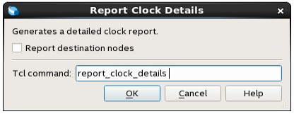
- In the Task pane, under Clock Reports, double-click Report Clock Details.
Figure 31. Chip Planner Task PaneFigure 32. Report Clock Details

- Click OK.
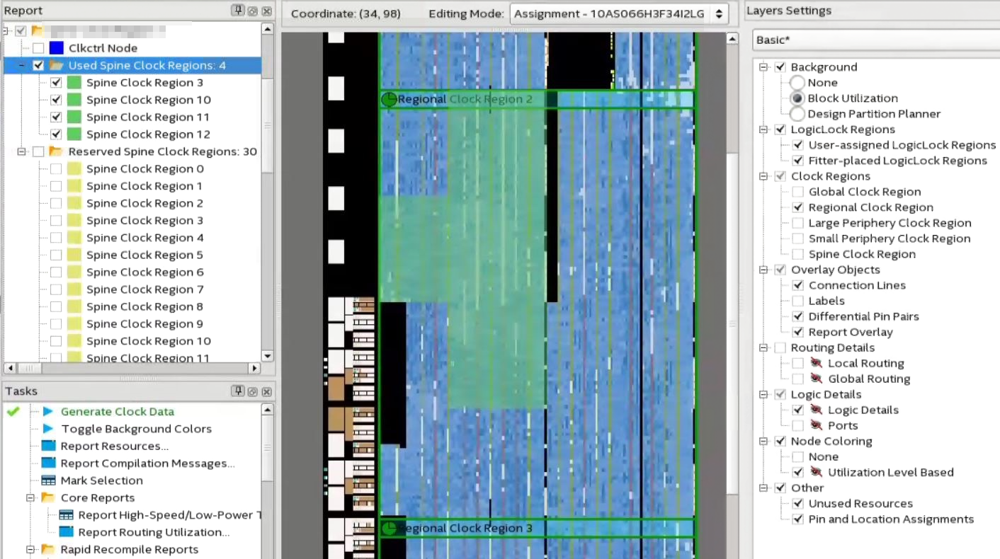
The Report pane generates the Clock folder.
- Expand the Clock folder and select Used spine clock regions to highlight on the Chip planner.
- In the Layers Settings pane, turn on Regional/Periphery clock region to see whether used spine clock regions are within.
Figure 33. Clock Highlight in Chip PlannerThis example uses a Regional clock Region instead of a global signal.
