Visible to Intel only — GUID: vat1574883297709
Ixiasoft
1. About the P-tile Avalon® Intel® FPGA IPs for PCI Express
2. IP Architecture and Functional Description
3. Advanced Features
4. Interfaces
5. Parameters
6. Testbench
7. Troubleshooting/Debugging
8. P-tile Avalon® Streaming Intel FPGA IP for PCI Express* User Guide Archives
9. Document Revision History for the P-Tile Avalon® Streaming Intel® FPGA IP for PCI Express* User Guide
A. Configuration Space Registers
B. Root Port Enumeration
C. Implementation of Address Translation Services (ATS) in Endpoint Mode
D. Packets Forwarded to the User Application in TLP Bypass Mode
E. Using the Avery BFM for Intel P-Tile PCI Express Gen4 x16 Simulations
F. Bifurcated Endpoint Support for Independent Warm Resets
G. Margin Masks for the P-Tile Avalon Streaming Intel FPGA IP for PCI Express
3.2.2.5.1. VirtIO Common Configuration Capability Register (Address: 0x012)
3.2.2.5.2. VirtIO Common Configuration BAR Indicator Register (Address: 0x013)
3.2.2.5.3. VirtIO Common Configuration BAR Offset Register (Address: 0x014)
3.2.2.5.4. VirtIO Common Configuration Structure Length Register (Address 0x015)
3.2.2.5.5. VirtIO Notifications Capability Register (Address: 0x016)
3.2.2.5.6. VirtIO Notifications BAR Indicator Register (Address: 0x017)
3.2.2.5.7. VirtIO Notifications BAR Offset Register (Address: 0x018)
3.2.2.5.8. VirtIO Notifications Structure Length Register (Address: 0x019)
3.2.2.5.9. VirtIO Notifications Notify Off Multiplier Register (Address: 0x01A)
3.2.2.5.10. VirtIO ISR Status Capability Register (Address: 0x02F)
3.2.2.5.11. VirtIO ISR Status BAR Indicator Register (Address: 0x030)
3.2.2.5.12. VirtIO ISR Status BAR Offset Register (Address: 0x031)
3.2.2.5.13. VirtIO ISR Status Structure Length Register (Address: 0x032)
3.2.2.5.14. VirtIO Device Specific Capability Register (Address: 0x033)
3.2.2.5.15. VirtIO Device Specific BAR Indicator Register (Address: 0x034)
3.2.2.5.16. VirtIO Device Specific BAR Offset Register (Address 0x035 )
3.2.2.5.17. VirtIO Device Specific Structure Length Register (Address: 0x036)
3.2.2.5.18. VirtIO PCI Configuration Access Capability Register (Address: 0x037)
3.2.2.5.19. VirtIO PCI Configuration Access BAR Indicator Register (Address: 0x038)
3.2.2.5.20. VirtIO PCI Configuration Access BAR Offset Register (Address: 0x039)
3.2.2.5.21. VirtIO PCI Configuration Access Structure Length Register (Address: 0x03A)
3.2.2.5.22. VirtIO PCI Configuration Access Data Register (Address: 0x03B)
4.1. Overview
4.2. Clocks and Resets
4.3. Serial Data Interface
4.4. Avalon-ST Interface
4.5. Hard IP Status Interface
4.6. Interrupt Interface
4.7. Error Interface
4.8. Hot Plug Interface (RP Only)
4.9. Power Management Interface
4.10. Configuration Output Interface
4.11. Configuration Intercept Interface (EP Only)
4.12. Hard IP Reconfiguration Interface
4.13. PHY Reconfiguration Interface
4.14. Page Request Service (PRS) Interface (EP Only)
4.4.1. TLP Header and Data Alignment for the Avalon-ST RX and TX Interfaces
4.4.2. Avalon® -ST RX Interface
4.4.3. Avalon® -ST RX Interface rx_st_ready Behavior
4.4.4. RX Flow Control Interface
4.4.5. Avalon® -ST TX Interface
4.4.6. Avalon® -ST TX Interface tx_st_ready Behavior
4.4.7. TX Flow Control Interface
4.4.8. Tag Allocation
5.2.3.1. Device Capabilities
5.2.3.2. VirtIO Parameters
5.2.3.3. Link Capabilities
5.2.3.4. Legacy Interrupt Pin Register
5.2.3.5. MSI Capabilities
5.2.3.6. MSI-X Capabilities
5.2.3.7. Slot Capabilities
5.2.3.8. Latency Tolerance Reporting (LTR)
5.2.3.9. Process Address Space ID (PASID)
5.2.3.10. Device Serial Number Capability
5.2.3.11. Page Request Service (PRS)
5.2.3.12. Access Control Service (ACS) Capabilities
5.2.3.13. Power Management
5.2.3.14. Vendor Specific Extended Capability (VSEC) Registers
5.2.3.15. TLP Processing Hints (TPH)
5.2.3.16. Address Translation Services (ATS) Capabilities
6.3.5.1. ebfm_barwr Procedure
6.3.5.2. ebfm_barwr_imm Procedure
6.3.5.3. ebfm_barrd_wait Procedure
6.3.5.4. ebfm_barrd_nowt Procedure
6.3.5.5. ebfm_cfgwr_imm_wait Procedure
6.3.5.6. ebfm_cfgwr_imm_nowt Procedure
6.3.5.7. ebfm_cfgrd_wait Procedure
6.3.5.8. ebfm_cfgrd_nowt Procedure
6.3.5.9. BFM Configuration Procedures
6.3.5.10. BFM Shared Memory Access Procedures
6.3.5.11. BFM Log and Message Procedures
6.3.5.12. Verilog HDL Formatting Functions
6.3.5.11.1. ebfm_display Verilog HDL Function
6.3.5.11.2. ebfm_log_stop_sim Verilog HDL Function
6.3.5.11.3. ebfm_log_set_suppressed_msg_mask Task
6.3.5.11.4. ebfm_log_set_stop_on_msg_mask Verilog HDL Task
6.3.5.11.5. ebfm_log_open Verilog HDL Function
6.3.5.11.6. ebfm_log_close Verilog HDL Function
A.3.1. Intel-Defined VSEC Capability Header (Offset 00h)
A.3.2. Intel-Defined Vendor Specific Header (Offset 04h)
A.3.3. Intel Marker (Offset 08h)
A.3.4. JTAG Silicon ID (Offset 0x0C - 0x18)
A.3.5. User Configurable Device and Board ID (Offset 0x1C - 0x1D)
A.3.6. General Purpose Control and Status Register (Offset 0x30)
A.3.7. Uncorrectable Internal Error Status Register (Offset 0x34)
A.3.8. Uncorrectable Internal Error Mask Register (Offset 0x38)
A.3.9. Correctable Internal Error Status Register (Offset 0x3C)
A.3.10. Correctable Internal Error Mask Register (Offset 0x40)
Visible to Intel only — GUID: vat1574883297709
Ixiasoft
2.1.3. Reset
There is only one PERST# (pin_perst_n) pin on P-Tile. Therefore, toggling pin_perst_n will affect the entire P-Tile. If the P-Tile x16 port is bifurcated into two x8 Endpoints, toggling pin_perst_n will affect both x8 Endpoints. To reset each port individually, use the in-band mechanism such as Hot Reset and the Function-Level Reset (FLR). Following are the guidelines for implementing the P-Tile pin_perst_n reset signal:
- pin_perst_n is a "power good" indicator from the associated power domain (to which P-Tile is connected). Also, it shall qualify that both the P-Tile refclk0 and refclk1 are stable. If one of the reference clocks becomes stable later, deassert pin_perst_n after this reference clock becomes stable.
- pin_perst_n assertion is required for proper Autonomous P-Tile functionality. In Autonomous mode (enabled by default), P-Tile can successfully link up upon the release of pin_perst_n regardless of the FPGA fabric configuration and will send out CRS (Configuration Retry Status) until the FPGA fabric is configured and ready.
- Avoid performing a warm reset or triggering pin_perst_n during a functional-level reset or before the functional-level reset completion. Otherwise, the PCIe link may get stuck in reset after the warm reset and cannot recover until cold reset is initiated.
- The minimum interval requirement between two consecutive resets is 500 μs. This is applicable to PERST#, Independent PERST and hot reset. In other words, the minimum interval time required between a deassertion of PERST# or Independent PERST to the assertion of the next PERST# or Independent PERST is 500 μs.
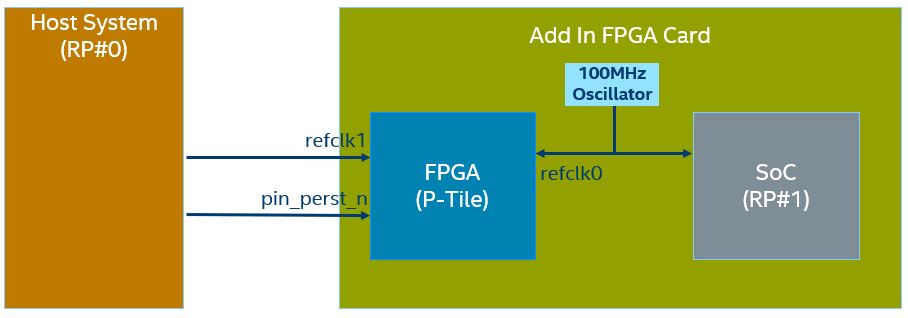
The following is an example where a single PERST# (pin_perst_n) is driven with independent refclk0 and refclk1. In this example, the add-in card (FPGA and Soc) is powered up first. P-Tile refclk0 is fed by the on-board free-running oscillator. P-Tile refclk1 driven by the Host becomes stable later. Hence, the PERST# is connected to the Host.
Figure 5. Single PERST# Connection in Bifurcated 2x8 Mode

