Board Developer Center
The FPGA Board Developer Center provides resources related to board-level design specifically for FPGAs. The goal is to help you successfully develop printed circuit boards (PCBs) using Agilex™ 7, Agilex™ 5, Agilex™ 3, Stratix® 10, Arria® 10, Cyclone® 10 GX, Cyclone® 10 LP, MAX® 10, Arria® V, Cyclone® V, MAX® V, Cyclone® IV devices. For Agilex™ devices, refer to the dedicated Agilex board journey resources listed below.
Board Design Journeys for Agilex™ 7, Agilex™ 5, and Agilex™ 3 Devices
Design Hubs provide a Step-by-Step Guided Journeys for standard development flows surfacing the key critical resources and documentation.
1. Design Considerations
Using Engineering Sample (ES) Devices
If you are designing a board using an engineering sample (ES) devices, please contact your Altera® sales representative or file an Intel® Premium Support case to get the latest board design guidelines for ES parts.
Board Design Guidelines for FPGAs
Topic |
Description |
|---|---|
The Board Design Solution Center provides resources related to board design for FPGAs. The goal is to help you implement successful high-speed PCBs that integrate FPGAs and other elements. |
|
This application note provides the recommended PCB design guidelines for some of the more complex package options offered for Altera programmable devices. Designers should also refer to the board design guidelines that are documented for the specific device family. |
|
Each FPGA family has its own pin connection guidelines. These guidelines are only recommendations by Altera. It is the responsibility of the designer to apply simulation results to the design and verify proper device functionality. |
|
Altera provides FPGA schematic review worksheets intended to help you review your schematic and adhere to the Altera guidelines. These worksheets are based on the respective device pin connection guidelines and other referenced documentation applicable to board-level pin connections that need to be considered when you finalize your schematic. |
Power Tree
Estimate the power consumption of the device and the decoupling networks that are required.
Topic |
Description |
|---|---|
The Altera power analysis tools, including early power estimators and the Quartus® Prime software Power Analyzer, give you the ability to estimate power consumption from early design concept through design implementation. As you provide more details about your design characteristics, estimation accuracy is improved with Power Analyzer technology. |
|
The PDN design tool provides a fast, accurate, and interactive way to determine the right number of decoupling capacitors for optimal cost and performance trade-offs. |
On-Chip Debug
Plan for system-level debug to assist in board bring-up and checkout.
Topic |
Description |
|---|---|
Altera provides a portfolio of on-chip debugging tools. The on-chip debugging tools allow real-time capture of internal nodes in your design to help you verify your design quickly without the use of external equipment. |
|
Altera provides boundary-scan description language (BSDL) files for IEEE Standard 1149.1, IEEE Standard 1149.6, and IEEE Standard 1532 specifications. BSDL files provide a syntax that allows the device to run boundary-scan test (BST) and in-system programmability (ISP). |
2. Learning Resources and Prerequisites
Create Your My Intel Account
- Create your My Intel account from the My Intel page.
- Your My Intel account allows you to file a service request, register for a class, download software, access resources, training courses, and much more.
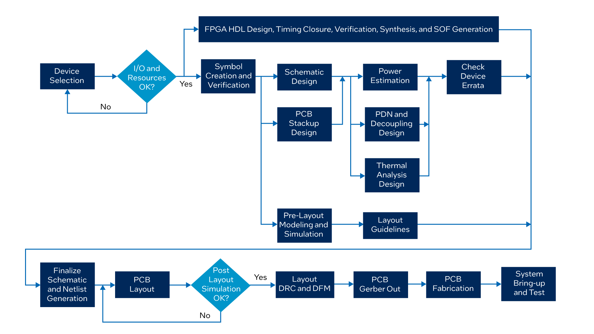
Design Flow
This figure shows the typical design flow using an FPGA or SoC FPGA. For more detailed explanation on each step, refer to the AN 597 Getting Started Flow for Board Designs.
Foundational Learning: Training Classes
Resource |
Description |
|---|---|
A starting place to quickly understand and use Altera® products, collateral, and resources. |
|
You have several options for software download, software updates, and additional device support. The option you choose depends on your download speed, design requirements, and installation methods. |
|
FPGA Technical Training offers training to help you sharpen your competitive edge. Take advantage of the interactivity of one of our instructor-led/virtual classroom courses, or the flexibility and convenience of an online course today. |
3. Getting Started
Component Selection
Topic |
Description |
|---|---|
The power tree illustrates the main power supply flow through a tree of power converters that convert the main power supply to the voltage and current required to drive various loads. Every FPGA design has unique power consumption requirements that require a unique power tree. |
|
This white paper discusses how to identify the various rails associated with Altera® devices, analyze the power requirements, and select the appropriate voltage regulator modules. This white paper also walks through a practical design example. |
|
Many of today’s FPGAs and SoCs have multiple power rails that need to be turned on in a specific order and monitored during runtime to ensure proper device operation. |
|
Altera provides solutions for a host of mainstream SDRAM and SRAM memory protocols as well as serial memory technologies, such as Hybrid Memory Cube (HMC) and Bandwidth Engine. Our memory interface solutions include high-performance memory controller options, memory PHY options, and multi-port front-end options. |
Schematic
Topic |
Description |
|---|---|
View the PCB footprint libraries and symbols for Cadence Capture CIS and Allegro Design Entry HDL (Allegro DE-HDL). |
|
View the PCB footprint libraries for Mentor Graphics PCB design tools. |
|
This website contains downloadable files listing FPGA pin-out descriptions. There are up to three types of files for each device: Portable Document Format files (.pdf), text files (.txt), and Microsoft* Excel files (.xls). |
|
This website provides the recommended pin connections for each device. Note: You need to apply simulation results to the design to verify proper device functionality. |
|
This website contains information on power analysis and estimation. Power analysis and early power estimators give you the ability to estimate power consumption from early design concept through design implementation. |
|
This website contains information on power distribution network (PDN) design. For each power supply, you must choose a network of bulk and ceramic decoupling capacitors. While you can use SPICE simulation to simulate the circuit, the PDN design tool provides a fast, accurate, and interactive way to determine the right number of decoupling capacitors for optimal cost and performance trade-offs. |
|
This website provides information on thermal management. Thermal management is an important design consideration. Altera® device packages are designed to minimize thermal resistance and maximize power dissipation. Some applications dissipate more power and will require external thermal solutions, including heat sinks. |
|
This page contains links to thermal resistance and package details for all device families. |
|
This website provides schematic review worksheets to help you review your schematic and adhere to design guidelines. |
Simulation
Topic |
Description |
|---|---|
This website contains information on transmission line effects, impedance mismatch, signal attenuation, crosstalk, and simultaneous switching outputs. |
|
This website contains information on SPICE kits for FPGAs. SPICE kits for FPGAs provide models that support a wide variety of I/O features across process, voltage, and temperature (PVT). |
|
This website contains information on IBIS models. The IBIS model allows the development of device models that preserve the proprietary nature of integrated circuit device designs, while at the same time providing information-rich models for signal integrity and electromagnetic compatibility (EMC) analysis. |
|
This document is a guideline for PCB layouts and designs associated with high-speed systems. |
|
This application note is for PCB designers planning to use high-speed transceiver-based devices and addresses two key design topics:
It also discusses the various strategies you can employ to compensate for the fiberglass weave effect, expands on existing knowledge, and lists various technical papers for additional information. |
|
| Net Length Reports | Net Length Reports provide the length and total delay of the package nets. Data is provided per pin for each device/package offered in table format. |
This website allows you to download the Board Skew Parameter Tool. The Board Skew Parameter Tool results are based on your simulated printed circuit board trace delays, the device package delays (if applicable), and the formulas from the External Memory Interfaces Parameters Handbook. The tool takes the input provided and calculates the skew parameters. |
Layout
Topic |
Description |
|---|---|
This document guides you in completing a board layout review using an FPGA. The technical content is divided into focus areas such as Power Planes and Stack Up, Critical Signals, Component Mounting, and Connectors. |
|
PCB Footprint Libraries for Cadence* Allegro PCB Tools. |
|
Mentor Graphics* Expedition Tool Footprint (physical package information) library. |
Board Bring-Up and Checkout
Topic |
Description |
|---|---|
Start here to learn about all the tools, examples, documentation, and training available to assist with PCB bring-up and help you debug your FPGA design. |
|
The IEEE 1149.1 BSDL files available on this website are used for pre- and post-configuration BST. |
|
The EMIF Toolkit lets you diagnose and debug calibration problems and produce margining reports for your external memory interface. |
|
The Transceiver Toolkit helps FPGA and board designers validate transceiver link signal integrity real time in a system and improve board bring-up time. Test for bit-error rate (BER) while simultaneously running multiple links at your target data rate to validate your board design. |
|
System Console is a flexible system-level debugging tool that helps designers quickly and efficiently debug their design while the design is running at full speed in an FPGA. System Console enables designers to send read and write system-level transactions into their Platform Designer (formerly Qsys) to help isolate and identify problems. It also provides a quick and easy way to check system clocks and monitor reset states, which can be particularly helpful during board bring-up. |
4. Developer Resources
Developer Resources
Topic |
Description |
|---|---|
Learn about signal integrity tools and models as well as power analysis and estimation. |
|
Package information including ordering codes, package acronym, leadframe material, lead finish (plating), JEDEC* outline reference, lead coplanarity, weight, moisture sensitivity level, and other special information. The thermal resistance information includes device pin count, package name, and resistance values. |
|
The External Memory Interface (EMIF) Handbook contains information and documentation regarding external memory interface design, intellectual property (IP) implementation and parameterization, simulation, debug, and much more. |
|
You can use this troubleshooter to help you identify possible causes to a failed FPGA configuration attempt. While this troubleshooter does not cover every possible case, it does identify a majority of problems encountered during configuration. |
|
A comprehensive collection of FPGA documentation, how-to videos, a community forum, online training courses, and a design store where customers can access an array of FPGA design examples. Hours of Engineer-to-Engineer videos provide a visual walkthrough of solving common design problems. |
5. PCB Manufacturing Resources
Resource |
Description |
Resource Type | Applicability |
|---|---|---|---|
| MAS Documents - Agilex™ 7 FPGAs | This Manufacturing Advantage Services (MAS) course shares Altera manufacturing recommendations to facilitate our customer’s manufacturing excellence. | Collection of assets | Agilex™ 7 Devices |
| MAS Documents - Agilex™ 5 FPGAs | This Manufacturing Advantage Services (MAS) course shares Altera manufacturing recommendations to facilitate our customer’s manufacturing excellence. |
Collection of assets | Agilex™ 5 Devices |
| MAS Documents - Agilex™ 3 FPGAs | This Manufacturing Advantage Services (MAS) course shares Altera manufacturing recommendations to facilitate our customer’s manufacturing excellence. | Collection of assets | Agilex™ 3 Devices |
| MAS Documents - Stratix® 10 FPGAs | This Manufacturing Advantage Services (MAS) course shares Altera manufacturing recommendations to facilitate our customer’s manufacturing excellence. | Collection of assets | Stratix® 10 Devices |
Guidelines for Handling J-Lead, QFP, BGA, FBGA, and Lidless FBGA Devices (AN71) |
This application note provides guidelines for handling J-Lead, Quad Flat Pack (QFP), and Ball-Grid Array (BGA, including FineLine BGA [FBGA] and lidless FBGA packaging) devices to preserve the quality of these devices during storage, shipment, and transfer and to ensure easier soldering. |
Collection of assets | J-Lead, QFP, BGA, FBGA, Lidless FBGA |
Thermal management and mechanical handling for FPGA TCFCBGA devices (AN657) |
This application note provides guidance on thermal management and mechanical handling of thermal composite flip chip ball-grid array (TCFCBGA) for Arria® V FPGA devices. |
Application Note |
TCFCBGA, Arria® V Devices |
Thermal management and mechanical handling for lidless flip chip ball-grid array (AN659) |
This application note provides guidance on thermal management and mechanical handling of lidless flip chip ball-grid array (FCBGA) for FPGA devices. |
Application Note |
Lidless FCBGA |
Guidelines for Handling Altera Wafer Level Chip Scale Package (WLCSP) (AN752) |
Proper care must be taken when handling Wafer Level Chip Scale Package (WLCSP) components. |
Application Note |
WLCSP |
Describes the differences between the conventional soldering and the lead-free soldering. Provides guidelines and recommendations for reflow soldering of Altera® lead-free devices. |
Application Note |
- |
|
Challenges in Manufacturing Reliable Lead-Free and RoHS-Compliant Components (White Paper) |
This white paper covers some of the modifications necessary and Altera® packaging solutions available to meet reliability and usability requirements for lead-free and RoHS-compliant products. |
White Paper |
PQFP, TQFP, BGA, FBGA, Flip-chip BGA |
Explore Other Developer Centers
For other design guidelines, visit the following Developer Centers:
- Embedded Software Developer Center - Contains guidance on how to design in an embedded environment with SoC FPGAs.
- FPGA Developer Center - Contains resources to complete your Altera® FPGA design.
- System Architect Developer Center - The System Architect Developer Center provides you with information on how Altera® FPGAs can add value to your system design.