Visible to Intel only — GUID: iin1659555625609
Ixiasoft
1. About the External Memory Interfaces Intel Agilex® 7 M-Series FPGA IP
2. Intel Agilex® 7 M-Series FPGA EMIF IP – Introduction
3. Intel Agilex® 7 M-Series FPGA EMIF IP – Product Architecture
4. Intel Agilex® 7 M-Series FPGA EMIF IP – End-User Signals
5. Intel Agilex® 7 M-Series FPGA EMIF IP – Simulating Memory IP
6. Intel Agilex 7 M-Series FPGA EMIF IP – DDR4 Support
7. Intel Agilex® 7 M-Series FPGA EMIF IP – DDR5 Support
8. Intel Agilex 7 M-Series FPGA EMIF IP – LPDDR5 Support
9. Intel Agilex® 7 M-Series FPGA EMIF IP – Timing Closure
10. Intel Agilex® 7 M-Series FPGA EMIF IP – Controller Optimization
11. Intel Agilex® 7 M-Series FPGA EMIF IP – Debugging
12. Document Revision History for External Memory Interfaces Intel Agilex® 7 M-Series FPGA IP User Guide
3.1.1. Intel Agilex® 7 M-Series EMIF Architecture: I/O Subsystem
3.1.2. Intel Agilex® 7 M-Series EMIF Architecture: I/O SSM
3.1.3. Intel Agilex® 7 M-Series EMIF Architecture: I/O Bank
3.1.4. Intel Agilex® 7 M-Series EMIF Architecture: I/O Lane
3.1.5. Intel Agilex® 7 M-Series EMIF Architecture: Input DQS Clock Tree
3.1.6. Intel Agilex® 7 M-Series EMIF Architecture: PHY Clock Tree
3.1.7. Intel Agilex® 7 M-Series EMIF Architecture: PLL Reference Clock Networks
3.1.8. Intel Agilex® 7 M-Series EMIF Architecture: Clock Phase Alignment
6.2.4.1. Address and Command Pin Placement for DDR4
6.2.4.2. DDR4 Data Width Mapping
6.2.4.3. General Guidelines
6.2.4.4. x4 DIMM Implementation
6.2.4.5. Specific Pin Connection Requirements
6.2.4.6. Command and Address Signals
6.2.4.7. Clock Signals
6.2.4.8. Data, Data Strobes, DM/DBI, and Optional ECC Signals
6.3.5.1. Single Rank x 8 Discrete (Component) Topology
6.3.5.2. Single Rank x 16 Discrete (Component) Topology
6.3.5.3. ADDR/CMD Reference Voltage/RESET Signal Routing Guidelines for Single Rank x 8 and Single Rank x 16 Discrete (Component) Topologies
6.3.5.4. Skew Matching Guidelines for DDR4 Discrete Configurations
6.3.5.5. Power Delivery Recommendations for DDR4 Discrete Configurations
6.3.5.6. Intel Agilex® 7 M-Series EMIF Pin Swapping Guidelines
Visible to Intel only — GUID: iin1659555625609
Ixiasoft
6.2.4.3. General Guidelines
Observe the following general guidelines when placing pins for your Intel Agilex® 7 M-Series external memory interface.
- Ensure that the pins of a single external memory interface reside on the same edge I/O.
- The address and command pins and their associated clock pins in the address and command bank must follow a fixed pin-out scheme, as defined in the table in the Address and Command Pin Placement for DDR4 topic.
- Not every byte lane can function as an address and command lane or a data lane. The pin assignment must adhere to the DDR4 data width mapping defined in DDR4 Data Width Mapping .
- A byte lane must not be used by both address and command pins and data pins.
- An I/O 96 bank cannot be used for more than one interface – meaning that two sub-banks belonging to two different EMIF interfaces are not permitted.
- Sharing of byte lanes within a sub-bank for two different interfaces is not permitted; you can assign byte lanes within a sub-bank to one EMIF interface only.
- Any pin in the same bank that is not used by an external memory interface may not be available for use as a general purpose I/O pin.
- When the network-on-a-chip (NoC) is used, the use of INIU may block the byte lane in the I/O bank adjacent to the sector where the INIU is located:
- INIU 0 blocks the access for BL 4, 5 and 6 (P48 to P83).
- INIU 1 blocks the access to the fabric AXI command/control port for the primary/secondary controller in the same I/O bank, making the hard controller unavailable for EMIF purposes.
- INIU 2 blocks the access for BL0,1,2,3 (P0 to P47).
- When the network-on-a-chip (NoC) is used, the use of INIU may block the byte lane in the I/O bank adjacent to the sector where the INIU is located:
- All address and command pins and their associated clock pins (CK and CK#) must reside within a single sub-bank. Refer to the table in DDR4 Data Width Mapping for the supported address and command and data lane placements for DDR4.
- An external memory interface can occupy one or more banks on the same edge. When an interface must occupy multiple banks, ensure the following:
- That the banks are adjacent to one another.
- That you used only the supported data width mapping as defined in the table in DDR4 Data Width Mapping . Be aware that not every byte lane can be used as an address and command lane or a data lane.
Figure 11. x72 DDR4 Pin Placement using Bank 2C and 2D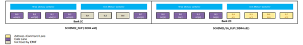
- Place read data groups according to the DQS grouping in the pin table and the Pin Planner. Read data strobes (such as DQS and DQS#) must reside at physical pins capable of functioning as DQS/CQ and DQSn/CQn for a specific read data group size. You must place the associated read data pins (such as DQ and Q), within the same group.
Note: For DDR4 interfaces with x4 components, you can use the strobe pins with either of the upper or lower DQ nibbles that are placed within a x8 DQS group in an I/O lane. You must place the DQ pins and associated strobes entirely in either the upper or lower half of a 12-bit bank sub-group.Consult the pin table for your device to identify the association between DQ pins and DQS pins for x4 mode operation. Additional restrictions apply for x4/x8 DIMM interoperability.
- One of the sub-banks in the device (typically the left sub-bank within corner Bank 3A) may not be available if you use certain device configuration schemes. For some schemes, there may be one byte lane available for EMIF data group:
- AVST-8 – This is contained entirely within the SDM, therefore all lanes of sub-bank 3A can be used by the external memory interface.
- AVST-32 – Byte lanes 4, 5, 6, and 7 are all effectively occupied and are not usable by the external memory interface.
- AVST-16 – Byte lanes 6 contains SDM_DATA[25:16], and is not used by AVSTx16. However, the external memory interface cannot use byte lane 6 when byte lanes 4 and 5 are not usable for EMIF purposes.