Visible to Intel only — GUID: fwh1658521143168
Ixiasoft
1. About the External Memory Interfaces Intel Agilex® 7 M-Series FPGA IP
2. Intel Agilex® 7 M-Series FPGA EMIF IP – Introduction
3. Intel Agilex® 7 M-Series FPGA EMIF IP – Product Architecture
4. Intel Agilex® 7 M-Series FPGA EMIF IP – End-User Signals
5. Intel Agilex® 7 M-Series FPGA EMIF IP – Simulating Memory IP
6. Intel Agilex 7 M-Series FPGA EMIF IP – DDR4 Support
7. Intel Agilex® 7 M-Series FPGA EMIF IP – DDR5 Support
8. Intel Agilex 7 M-Series FPGA EMIF IP – LPDDR5 Support
9. Intel Agilex® 7 M-Series FPGA EMIF IP – Timing Closure
10. Intel Agilex® 7 M-Series FPGA EMIF IP – Controller Optimization
11. Intel Agilex® 7 M-Series FPGA EMIF IP – Debugging
12. Document Revision History for External Memory Interfaces Intel Agilex® 7 M-Series FPGA IP User Guide
3.1.1. Intel Agilex® 7 M-Series EMIF Architecture: I/O Subsystem
3.1.2. Intel Agilex® 7 M-Series EMIF Architecture: I/O SSM
3.1.3. Intel Agilex® 7 M-Series EMIF Architecture: I/O Bank
3.1.4. Intel Agilex® 7 M-Series EMIF Architecture: I/O Lane
3.1.5. Intel Agilex® 7 M-Series EMIF Architecture: Input DQS Clock Tree
3.1.6. Intel Agilex® 7 M-Series EMIF Architecture: PHY Clock Tree
3.1.7. Intel Agilex® 7 M-Series EMIF Architecture: PLL Reference Clock Networks
3.1.8. Intel Agilex® 7 M-Series EMIF Architecture: Clock Phase Alignment
6.2.4.1. Address and Command Pin Placement for DDR4
6.2.4.2. DDR4 Data Width Mapping
6.2.4.3. General Guidelines
6.2.4.4. x4 DIMM Implementation
6.2.4.5. Specific Pin Connection Requirements
6.2.4.6. Command and Address Signals
6.2.4.7. Clock Signals
6.2.4.8. Data, Data Strobes, DM/DBI, and Optional ECC Signals
6.3.5.1. Single Rank x 8 Discrete (Component) Topology
6.3.5.2. Single Rank x 16 Discrete (Component) Topology
6.3.5.3. ADDR/CMD Reference Voltage/RESET Signal Routing Guidelines for Single Rank x 8 and Single Rank x 16 Discrete (Component) Topologies
6.3.5.4. Skew Matching Guidelines for DDR4 Discrete Configurations
6.3.5.5. Power Delivery Recommendations for DDR4 Discrete Configurations
6.3.5.6. Intel Agilex® 7 M-Series EMIF Pin Swapping Guidelines
Visible to Intel only — GUID: fwh1658521143168
Ixiasoft
9.2. Optimizing Timing
The Intel® Quartus® Prime software offers several advanced features that you can use to assist in meeting core timing requirements.
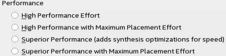
- On the Assignments menu, click Settings. In the Category list, click Compiler Settings. Under Optimization mode, select one of the Performance options.
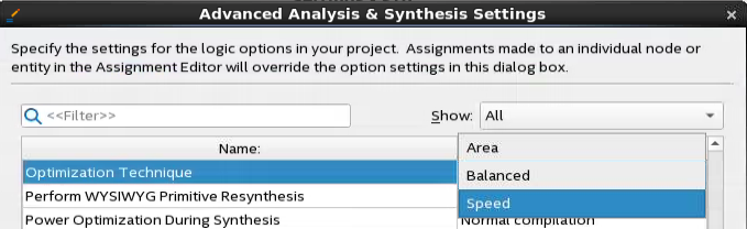
- On the Assignments menu, click Settings. In the Category list, click Compiler Settings > Advanced Settings (Synthesis). For Optimization Technique, select Speed.
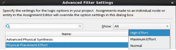
- On the Assignments menu, click Settings. In the Category list, click Compiler Settings > Advanced Settings (Fitter). For Physical Placement Effort, select High Effort or Maximum Effort. The High and Maximum effort settings take additional compilation time to further optimize placement.
- On the Assignments menu, click Settings. In the Category list, click Compiler Settings > Advanced Settings (Fitter). For Placement Effort Multiplier, select a number higher than the preset value of 1.0. A higher value increases CPU time, but may improve placement quality.
