6.3. Thermal Page and Thermal Design Parameters
The maximum junction temperature rating of all Agilex™ 7 dies is 100°C unless stated otherwise in the documentation.
Inputs to the Intel® FPGA Power and Thermal Calculator (PTC) Thermal Page
In the Intel® FPGA Power and Thermal Calculator (PTC), you must select the type of analysis that you want to perform, and provide the system thermal parameters.
With the Thermal page active, you must choose appropriate settings for Calculation Mode and Recommended margin:
- Calculation Mode. Choose one of the following:
- Use a constant junction temperature.
- This mode assumes that all the dies are at the same fixed, constant temperature. The power calculated in the constant junction temperature mode is not representative of actual power during use. It is unlikely that all components of the die are at uniform temperature during normal operation. For more representative power, use the other calculation modes that utilize the thermal calculator.
- Enter the junction temperature for this mode, on the Main page or the Thermal page.
- Find a cooling solution for a maximum junction temperature.
- In this mode the PTC finds the TCASE, cooling solution, ΨCA, and power of all the dies, while no die can exceed the entered maximum TJ.
- Enter the maximum TJ and ambient temperature suitable for the design. (For our example, assume a maximum TJ of 95°C, and an ambient temperature of 50°C.
- Find a maximum junction temperature for a cooling solution.
- In this mode the PTC finds the thermal parameters for a known cooling solution and ambient temperature.
- Enter the ΨCA and ambient temperature.
- Find an ambient temperature for a cooling solution.
- In this mode the PTC finds the ambient temperature which can allow the specified cooling solution to meet the junction temperature target and maximum TJ.
- Enter the maximum TJ suitable to the design and ΨCA.
- Use a constant junction temperature.
- Apply recommended margin. Choose one of the following:
- Set this field to yes if the power model status in the main page is not final. Added margins are set very conservatively at 25% extra power. Consult your Intel Field Application Engineer (FAE) before adding margin power to your design.
- In general, it is good engineering practice to add some margin very early in the design cycle when the RTL design is not yet available, and only the PTC is used for evaluation. You can do this by applying, for example, 5% higher toggle rates or clock frequencies to various logic settings to increase the core power. Transceiver function, power, and placement are usually stable and should not change through the course of the project, therefore no additional margin need apply there.
Intel® FPGA Power and Thermal Calculator (PTC) Thermal Page Outputs
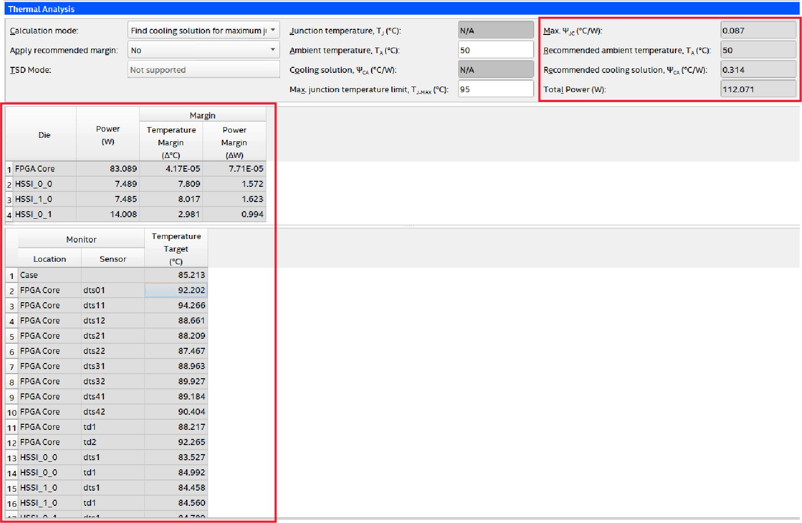
The following figure shows the PTC Thermal page for the PCIe board example, with output fields circled in red.
Figure 8. Intel® FPGA Power and Thermal Calculator (PTC) Thermal Page - Outputs Marked in Red


The thermal page outputs are as follows:
- Die power is the thermal power dissipated by each die, and is used for the thermal analysis.
- Temperature margin for each die. In the case of our example, this is calculated relative to a designated maximum TJ of 95°C. Often, one or more dies may have no margin, because the solution is calculated for the specified maximum TJ. In this example, the core fabric is operating at 95°C. The HSSI_0_0 transceiver is operating at 95-5.2= 89.8°C and HSSI_0 transceiver is operating at 93.3°C.
- Power margin, The PTC calculates the power margin for each die. That is the power for resources that can be added before the maximum TJ is exceeded under the same cooling condition. This is only an approximate indication, as the exact value varies depending on the specific subsystem to which the power is allocated. Any increase or decrease in total power causes a change in the cooling solution requirement.
- Max ΨjC is the thermal resistance of the die with the highest temperature. In this example, the maximum resistance belongs to the core fabric die, because it has the highest junction temperature. To check the results: TJ-MAX = TCASE+ TTP × ΨjC =88.3 +(58+7.8+7.9) × 0.091= 95° C.
- ΨCA is the maximum thermal resistance of the cooling solution that satisfies the cooling requirement. In this case of our example, TJ= TAMBIENT + TTP × (ΨjC +ΨCA)=50+73.6*(+0.091+0.519)=95°C.
- TCASE is the temperature at the top center of the FPGA lid and may not necessarily be hottest temperature. In a computational fluid dynamic (CFD) analysis, this temperature is the best indication of whether the cooling solution meets the design requirements. Intel recommends putting a sensor in the center of the integrated heat spreader (IHS) if the compact thermal model (CTM) does not come with one.
- Die monitor temperatures, are the temperatures at the FPGA temperature sensors when the system is operating. These sensors may not necessarily be in the hottest locations, and therefore might report values less than the maximum value in the design. If these thresholds are exceeded, it indicates that extra cooling is required, otherwise the targeted design goal may be exceeded.