Visible to Intel only — GUID: nzt1642154563029
Ixiasoft
1. Quick Start Guide
2. Design Example: Single IP Core Instantiation
3. Design Example: Single IP Core Instantiation with Precision Time Protocol
4. Design Example: Single IP Core Instantiation with Auto-Negotiation and Link Training
5. Design Example: Multiple IP Core Instantiation
6. Design Example: Two Separate Instances of Auto-Negotiation and Link Training and Ethernet IP Design
7. F-Tile Ethernet Intel® FPGA Hard IP Design Example User Guide Archives
8. Document Revision History for the F-Tile Ethernet Intel FPGA Hard IP Design Example User Guide
Visible to Intel only — GUID: nzt1642154563029
Ixiasoft
1.5. Compiling and Configuring the Design Example in Hardware
To compile the hardware design example and configure it on your Intel device, follow these steps:
- Ensure hardware design example generation is complete.
- In the Quartus® Prime Pro Edition software, navigate to the Quartus® Prime project directory eth_f_0_example_design/hardware_test_design/.
- Open the Quartus® Prime project:
quartus eth_f_hw.qpf &
- On the Processing menu, click Start Compilation.
- After successful compilation, a .sof file is available in <design_example_directory>/hardware_test_design/output_files.
- Connect the Agilex 7 I-Series Transceiver-SoC Development Kit to the host computer.
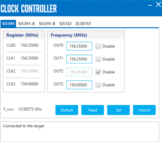
- Launch the Clock Controller application, which is part of the development kit.
Figure 9. Clock Controller
 Set new frequencies for the design example as following:
- Si5394 (U118), OUT3: Set to the value of i_refclk2pll 2 as 156.25MHz.
- On the Tools menu, click Programmer.
- In the Programmer, click Hardware Setup.
- Select a programming device.
- Select and add the Development Kit to which your Quartus® Prime Pro Edition session can connect.
- Ensure that Mode is set to JTAG.
- Select the device and click Add Device. The Programmer displays a block diagram of the connections between the devices on your board.
- In the row with your .sof, check the Program/Configure box for the .sof file.
- Click Start.
Note: If the System PLL fails to lock when the i_refclk2pll frequency is greater than 156.25MHz, please refer to the steps specified in Why do F-tile Reference and System PLL clocks Intel® FPGA IP fail to lock at specific frequencies? to resolve the issue.
2 The Clock Control GUI application cannot drive all the frequencies.