Visible to Intel only — GUID: nok1520732181938
Ixiasoft
Visible to Intel only — GUID: nok1520732181938
Ixiasoft
3.4.1. Hard Memory Controller
The hard memory controller implements efficient pipelining techniques and advanced dynamic command and data reordering algorithms to improve bandwidth usage and reduce latency, providing a high performance solution.
The controller architecture is modular and fits in a single I/O bank. The structure allows you to:
- Configure each I/O bank as either:
- A control path that drives all the address and command pins for the memory interface.
- A data path that drives up to 32 data pins for DDR-type interfaces.
- Place your memory controller in any location.
- Pack up multiple banks together to form memory interfaces of different widths up to 72 bits.
- Bypass the hard memory controller and use your own custom IP if required.

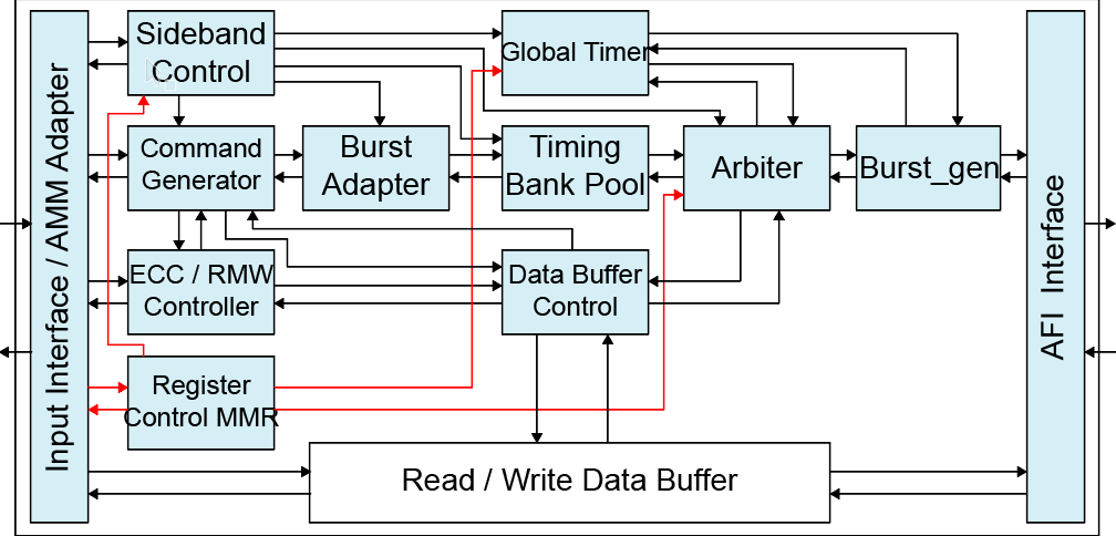
The hard memory controller consists of the following logic blocks:
- Core and PHY interfaces
- Main control path
- Data buffer controller
- Read and write data buffers
The core interface supports the Avalon® Memory-Mapped (Avalon-MM) interface. The interface communicates to the PHY using the Altera PHY Interface (AFI). The whole control path is split into the main control path and the data buffer controller.