Visible to Intel only — GUID: nik1412632490644
Ixiasoft
1.3.7. Connectors Optimization
Another component commonly found in the path of transceiver channels are backplane connectors and optical interface modules such as SFP+, XFP, and CFP2 among many others. For these components, the manufacturer may have specific design recommendations for the best connector performance, and the designer should follow those recommendations. If no recommendation is provided by the manufacturer, perform simulations to determine the best layout optimization. However, because most backplane and optical connector systems use press-fit through-hole via or surface mount pad technology respectively, the concept for optimization is very similar to that done for transparent via design and DC blocking capacitor compensation. The impact of impedance mismatch limits performance. For these cases, you can use the same methodology to optimize both the vias and surface mount pads in the connectors to better match the connector impedance to the 100-Ω trace impedance.


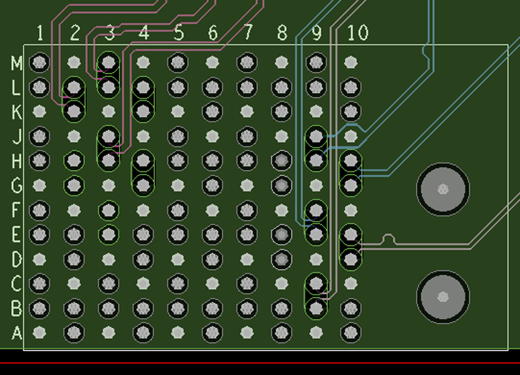
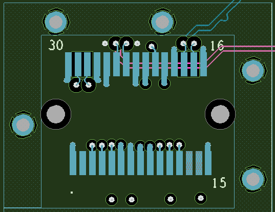
Notice that the via and surface mount pads show evidence of optimization such as increased via anti-pad size and plane cut-outs underneath the surface mount pads.