Visible to Intel only — GUID: nik1412632468992
Ixiasoft
1.3.1. BGA Channel Breakout
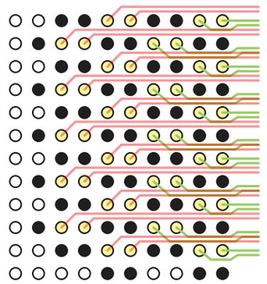
As the number of very high-speed transceiver pairs on FPGAs continue to increase, the complexity of the channel breakout design increases as well. Trace breakout can typically use either a single trace or dual trace topology between the BGA via grid.


In the single trace breakout, more layers are required to fully route all the TX and RX transceiver pairs because only one trace is routed between the BGA via grid per layer. Because there is ample space for a maximum trace width of up to 13.37 mils (assuming typical minimum trace-to-copper clearances of 4 mils for the recommended 18 mil via pad size and 39.37 mil via-to-via center pitch), the trace width and resulting characteristic impedance is easily made uniform throughout the trace route.
In the dual trace breakout, two traces are used to reduce layer count requirement, but their maximum trace width is limited to 4.68 mils because of the same trace-to-copper clearance requirements. Because high-speed transceiver traces are usually routed using trace widths of 6 to 8 mils (or more) to reduce the impact of skin effect losses at higher frequencies, the reduction of trace width to accommodate dual trace breakout effectively increases the trace impedance. However, this increase is offset by the reduction of the trace-to-trace separation in the differential pair, so the net impedance remains unchanged.
| Topology | Height from Reference Plane (H1/H2 in mils) | Er | Trace Width (W in mils) | Trace Separation (S in mils) | Diff Zo (Ω) |
|---|---|---|---|---|---|
| Stripline | 9/9 | 3.7 | 6 | 6.5 | 100 |
| Stripline | 9/9 | 3.7 | 4 | 4 | 101 |
Another benefit of the trace neck down is that the thinner trace width increases the trace inductance and helps to compensate for the higher capacitance of the BGA ball pad.