Visible to Intel only — GUID: nik1410905618754
Ixiasoft
Visible to Intel only — GUID: nik1410905618754
Ixiasoft
4.7.4. Read DMA Example
This example moves three data blocks from the system memory to the Avalon-MM address space. Host software running on an embedded CPU allocates the memory and creates the descriptor table in system memory.
This example uses the addresses in the Platform Designer design example, ep_g3x8_avmm256_integrated.qsys, available in the <install_dir>/ ip/altera/altera_pcie/altera_pcie_<dev>_ed/example_design/<dev> directory.
The following figures illustrate the location and size of the data blocks in the PCIe and Avalon-MM address spaces and the descriptor table format. In this example, the value of RD_TABLE_SIZE is 127.
Assume the descriptor table includes 128 entries. The status table precedes a variable number of descriptors in memory. The Read and Write Status and Descriptor Tables are at the address specified in the RC Read Descriptor Base Register and RC Write Descriptor Base Register, respectively.
- Calculate the memory allocation required:
- Each entry in the status table is 4 bytes. The 128 entries require 512 bytes of memory.
- Each descriptor is 32 bytes. The three descriptors require 96 bytes of memory.
The total memory allocation for the status and descriptor tables is 608 bytes. - Allocate 608 bytes of memory in the PCI Express address space.
The start address of the allocated memory in this example is 0xF000_0000. Program this address into the Root Complex Read Status and Descriptor Base Address Registers.
- Create the descriptor table in the PCI Express address space. Because the status table is stored before the descriptors, the first descriptor is stored at 0xF000_0000 + 0x200 = 0xF000_0200.
- Program 0x0000_0000 into the source address 0xF000_0204 in descriptor 0.
This is the upper 32 bits of the source address.
- Program 0x1000_0000 into the source address 0xF000_0200 in descriptor 0.
This is the lower 32 bits of the source address.
- Program 0x0000_0000 into the destination address 0xF000_020C in descriptor 0.
This is the upper 32 bits of the destination address.
- Program 0x5000_0000 into the destination address 0xF000_0208 in descriptor 0.
This is the lower 32 bits of the destination address.These four steps program the Avalon-MM destination address for the 64 KB block of memory into the Descriptor Table.
- Program 0x0000_4000 to 0xF000_0210 to transfer 16K dwords (64 KB), of data for descriptor ID 0.
- Program 0x0000_0000 into the source address 0xF000_0204 in descriptor 0.
- Repeat this procedure for the second data block:
- Program 0x0000_0000 to source address 0xF000_0224.
- Program 0x2000_0000 to source address 0xF000_0220.
- Program 0x0000_0000 to destination address 0xF000_022C.
- Program 0x0001_0000 to destination address 0xF000_0228.
- Program 0x0004_2000 to 0xF000_0230 to transfer 8K dwords (32 KB) of data for descriptor ID 1.
- Repeat this procedure for the third data block:
- Program 0x0000_0001 to source address 0xF000_0244.
- Program 0x2000_0000 to source address 0xF000_0240.
- Program 0x0000_0000 to destination address 0xF000_024C.
- Program 0x1000_0000 to destination address 0xF000_0248.
- Program 0x0008_1000 to 0xF000_0250 to transfer 4K dwords (16 KB) of data for descriptor ID 2.
The following figure shows the values in the Descriptor Table after programming completes.Figure 9. Descriptor Table Format - Program the DMA Descriptor Controller with the address of the status and descriptor table in the PCI Express system memory address space. When the DMA Descriptor Controller is internal, these registers are accessed through combined BAR0 and BAR1 because this example uses 64-bit addresses. The DMA read control registers start at offset 0x0000. The Write DMA control registers start at offset 0x0100
- Program 0x0000_0000 to offset 0x0000_0004.
This is the upper 32 bits of the PCIe system memory where the status and descriptor table is stored.
- Program 0xF000_0000 to offset 0x0000_0000.
This is the lower 32 bits of the address in PCIe memory that stores the status and descriptor tables. The Read DMA automatically adds an offset of 0x200 to this value to start the copy of the descriptors which follow the status table in memory.
- Program 0x0000_0000 to offset 0x0000_0004.
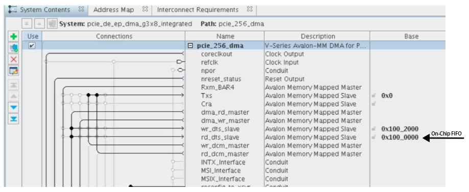
- Program the DMA Descriptor Controller with the on-chip FIFO address. This is the address to which the Descriptor Controller copies the status and descriptor table.
- Program 0x0000_0000 to offset 0x0000_000C
This is the upper 32 bits of the on-chip FIFO address in the Avalon-MM address domain.
- Program 0x0100_0000 to offset 0x0000_0008.
This is the lower 32 bits of the on-chip FIFO address. This is address of the internal on-chip FIFO that is a part of the Descriptor Controller as seen by the RX Master.Figure 10. Address of the On-Chip FIFO

- Program 0x0000_0000 to offset 0x0000_000C
- Program the Descriptor Controller RD_DMA_LAST_PTR register.
This step starts the DMA. It also specifies the status dword to be updated when the three descriptors complete.
-
To update a single done bit for the final descriptor, program 0x2 to offset 0x0000_0010. The Descriptor Controller processes all three descriptors and writes the done bit to 0xF000_0008 of the status table.
- To update the done bits for all three descriptors, program address 0x0000_0010 RD_DMA_LAST_PTR three times with the values 0, 1, and 2. The Descriptor Controller sets the done bits for addresses 0xF000_0000, 0xF000_0004, and 0xF000_0008. If the system returns Read Completions out-of-order, the Descriptor Controller may complete descriptors out of order. In such systems, you must use this method of requesting done status for each descriptor. Software must check for done status for every descriptor.
-