Visible to Intel only — GUID: aem1602789221139
Ixiasoft
1. Introduction
2. IP Architecture and Functional Description
3. Advanced Features
4. Interfaces
5. Parameters
6. R-tile Avalon® Streaming Intel® FPGA IP for PCI Express* User Guide Archives
7. Document Revision History for the R-tile Avalon® Streaming Intel FPGA IP for PCI Express User Guide
A. Configuration Space Registers
B. Root Port Enumeration
C. Implementation of Address Translation Services (ATS) in Endpoint Mode
D. Packets Forwarded to the User Application in TLP Bypass Mode
3.2.2.5.1. VirtIO Common Configuration Capability Register (Address: 0x012)
3.2.2.5.2. VirtIO Common Configuration BAR Indicator Register (Address: 0x013)
3.2.2.5.3. VirtIO Common Configuration BAR Offset Register (Address: 0x014)
3.2.2.5.4. VirtIO Common Configuration Structure Length Register (Address 0x015)
3.2.2.5.5. VirtIO Notifications Capability Register (Address: 0x016)
3.2.2.5.6. VirtIO Notifications BAR Indicator Register (Address: 0x017)
3.2.2.5.7. VirtIO Notifications BAR Offset Register (Address: 0x018)
3.2.2.5.8. VirtIO Notifications Structure Length Register (Address: 0x019)
3.2.2.5.9. VirtIO Notifications Notify Off Multiplier Register (Address: 0x01A)
3.2.2.5.10. VirtIO ISR Status Capability Register (Address: 0x02F)
3.2.2.5.11. VirtIO ISR Status BAR Indicator Register (Address: 0x030)
3.2.2.5.12. VirtIO ISR Status BAR Offset Register (Address: 0x031)
3.2.2.5.13. VirtIO ISR Status Structure Length Register (Address: 0x032)
3.2.2.5.14. VirtIO Device Specific Capability Register (Address: 0x033)
3.2.2.5.15. VirtIO Device Specific BAR Indicator Register (Address: 0x034)
3.2.2.5.16. VirtIO Device Specific BAR Offset Register (Address 0x035)
3.2.2.5.17. VirtIO Device Specific Structure Length Register (Address: 0x036)
3.2.2.5.18. VirtIO PCI Configuration Access Capability Register (Address: 0x037)
3.2.2.5.19. VirtIO PCI Configuration Access BAR Indicator Register (Address: 0x038)
3.2.2.5.20. VirtIO PCI Configuration Access BAR Offset Register (Address: 0x039)
3.2.2.5.21. VirtIO PCI Configuration Access Structure Length Register (Address: 0x03A)
3.2.2.5.22. VirtIO PCI Configuration Access Data Register (Address: 0x03B)
4.4.1. Avalon® Streaming Interface
4.4.2. Precision Time Measurement (PTM) Interface
4.4.3. Interrupt Interface
4.4.4. Hard IP Reconfiguration Interface
4.4.5. Error Interface
4.4.6. Completion Timeout Interface
4.4.7. Configuration Intercept Interface
4.4.8. Power Management Interface
4.4.9. Hard IP Status Interface
4.4.10. Page Request Services (PRS) Interface
4.4.11. Function-Level Reset (FLR) Interface
4.4.12. SR-IOV VF Error Flag Interface
4.4.13. General Purpose VSEC Interface
5.2.3.1. Device Capabilities
5.2.3.2. VirtIO Parameters
5.2.3.3. Link Capabilities
5.2.3.4. Legacy Interrupt Pin Register
5.2.3.5. MSI Capabilities
5.2.3.6. MSI-X Capabilities
5.2.3.7. Slot Capabilities
5.2.3.8. Latency Tolerance Reporting (LTR)
5.2.3.9. Process Address Space ID (PASID)
5.2.3.10. Device Serial Number Capability
5.2.3.11. Page Request Service (PRS)
5.2.3.12. Access Control Service (ACS)
5.2.3.13. Power Management
5.2.3.14. Vendor Specific Extended Capability (VSEC) Registers
5.2.3.15. TLP Processing Hints (TPH)
5.2.3.16. Address Translation Services (ATS) Capabilities
5.2.3.17. Precision Time Management (PTM)
Visible to Intel only — GUID: aem1602789221139
Ixiasoft
4.4.1.1. TLP Header and Data Alignment for the Avalon® streaming RX and TX Interfaces
The TLP prefix, header and data are sent and received on the Avalon® streaming TX and RX interfaces. There are four Avalon® streaming TX/RX interfaces corresponding to the four PCIe cores. The signal names on these interfaces are prefixed with "p0" for the x16 core, "p1" for the x8 core, "p2" for the x4_0 core and "p3" for the x4_1 core.
Each of these interfaces can contain up to four segments. The signal names for these segments are notated with *_st0_*, *_st1_*, *_st2_* and *_st3_*.
A Start of Packet (SOP) symbol demarcates the start of a packet. A command with or without data is terminated by an End of Packet (EOP) symbol. An EOP happening on the st0, st1, st2 or st3 segment implies that the last data with data valid = 1 is located on the corresponding data bus.
A command without data is qualified by a header valid indicator. A command with data is qualified by a data valid indicator. There is also a prefix valid indicator to qualify a TLP Prefix.
If a global valid signal is required for backward compatibility to P-tile, the header valid ORed with data valid will provide the global valid indicator.
This is defined to enable pipelined Header/Prefix and Data transfers to meet the bandwidth target. For example, while transferring the Data for one TLP, the Header and Prefix for the next TLP can also be transferred.
Figure 20. Generic TLP Format
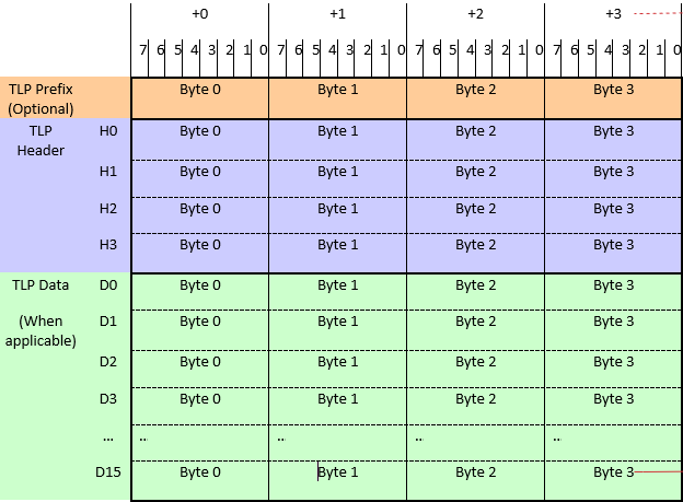
The Avalon® streaming Header and TLP Prefix bus packet format follows the TLP packet format as defined by the PCIe specification for Memory, Configuration and Message TLPs. Refer to Figure 21 and Figure 22 below for more details.
In the R-tile Parameter Editor, there is a checkbox labeled PCIe Header format (in the PCIe Avalon® Settings tab) that allows you to specify whether the Header will follow the Big Endian format or Little Endian format. If this checkbox is not enabled, the Header follows the Little Endian format as shown in Figure 21 (note that the diagram shows the Prefix, Header and Data for one segment of the Avalon® streaming interface, not the whole interface):
Figure 21. TLP Prefix, Header and Data when PCIe Header Format Checkbox is Disabled
If the PCIe Header format checkbox is enabled, the Header follows the Big Endian format as shown in Figure 22:
Figure 22. TLP Prefix, Header and Data when PCIe Header Format Checkbox is Enabled
| Configuration | Link Rate | Width Mode | Header | Data | Application Clock Frequency (MHz) |
|---|---|---|---|---|---|
| x16 | Gen5 | Double-Width | H3[127:0], H2[127:0], H1[127:0], H0[127:0] | D3[255:0], D2[255:0], D1[255:0], D0[255:0] | 400 - 500 |
| Gen4 | Double-Width | H3[127:0], H2[127:0], H1[127:0], H0[127:0] | D3[255:0], D2[255:0], D1[255:0], D0[255:0] | 250 - 300 | |
| Gen3 | Double-Width | H3[127:0], H2[127:0], H1[127:0], H0[127:0] | D3[255:0], D2[255:0], D1[255:0], D0[255:0] | 250 - 300 | |
| x8x8 | Gen5 | Double-Width | H1[127:0], H0[127:0] | D1[255:0], D0[255:0] | 400 - 500 |
| Gen4 | Double-Width | H1[127:0], H0[127:0] | D1[255:0], D0[255:0] | 250 - 300 | |
| Gen3 | Double-Width | H1[127:0], H0[127:0] | D1[255:0], D0[255:0] | 250 - 300 | |
| x4x4x4x4 | Gen5 | Double-width | H1[127:0], H0[127:0] | D1[127:0], D0[127:0] | 400 - 500 |
| Gen4 | Double-width | H1[127:0], H0[127:0] | D1[127:0], D0[127:0] | 250 - 300 | |
| Gen3 | Double-width | H1[127:0], H0[127:0] | D1[127:0], D0[127:0] | 250 - 300 |
Note:
- For the PCIe x16 configuration in double-width mode, the H2 TLP header is only allowed if H0 and H1 (also D0 and D1) have been used.
- Single-width modes are not available in the 21.4 release of Intel® Quartus® Prime.
- For x16 mode, an SOP can happen only on segment 0 (st0) or segment 2 (st2) for the TX Avalon streaming interface.