Visible to Intel only — GUID: luy1693244616234
Ixiasoft
1. About the External Memory Interfaces Agilex™ 7 M-Series FPGA IP
2. Agilex™ 7 M-Series FPGA EMIF IP – Introduction
3. Agilex™ 7 M-Series FPGA EMIF IP – Product Architecture
4. Agilex™ 7 M-Series FPGA EMIF IP – End-User Signals
5. Agilex™ 7 M-Series FPGA EMIF IP – Simulating Memory IP
6. Agilex™ 7 M-Series FPGA EMIF IP – DDR4 Support
7. Agilex™ 7 M-Series FPGA EMIF IP – DDR5 Support
8. Agilex™ 7 M-Series FPGA EMIF IP – LPDDR5 Support
9. Agilex™ 7 M-Series FPGA EMIF IP – Timing Closure
10. Agilex™ 7 M-Series FPGA EMIF IP – Controller Optimization
11. Agilex™ 7 M-Series FPGA EMIF IP – Debugging
12. Agilex™ 7 FPGA EMIF IP - Mailbox Support
13. Document Revision History for External Memory Interfaces Agilex™ 7 M-Series FPGA IP User Guide
3.1.1. Agilex™ 7 M-Series EMIF Architecture: I/O Subsystem
3.1.2. Agilex™ 7 M-Series EMIF Architecture: I/O SSM
3.1.3. Agilex™ 7 M-Series EMIF Architecture: I/O Bank
3.1.4. Agilex™ 7 M-Series EMIF Architecture: I/O Lane
3.1.5. Agilex™ 7 M-Series EMIF Architecture: Input DQS Clock Tree
3.1.6. Agilex™ 7 M-Series EMIF Architecture: PHY Clock Tree
3.1.7. Agilex™ 7 M-Series EMIF Architecture: PLL Reference Clock Networks
3.1.8. Agilex™ 7 M-Series EMIF Architecture: Clock Phase Alignment
3.1.9. User Clock in Different Core Access Modes
4.1. IP Interfaces for Agilex 7 M-Series External Memory Interfaces (EMIF) IP - DDR4 Component
4.2. IP Interfaces for Agilex 7 M-Series External Memory Interfaces (EMIF) IP - DDR4 DIMM
4.3. IP Interfaces for Agilex 7 M-Series External Memory Interfaces (EMIF) IP - DDR5 Component
4.4. IP Interfaces for Agilex 7 M-Series External Memory Interfaces (EMIF) IP - DDR5 DIMM
4.5. IP Interfaces for Agilex 7 M-Series External Memory Interfaces (EMIF) IP - LPDDR5
4.1.1. s0_axi4_clock_in for Agilex 7 M-Series External Memory Interfaces (EMIF) IP - DDR4 Component
4.1.2. s0_axi4_clock_out for Agilex 7 M-Series External Memory Interfaces (EMIF) IP - DDR4 Component
4.1.3. s0_axi4_ctrl_ready for Agilex 7 M-Series External Memory Interfaces (EMIF) IP - DDR4 Component
4.1.4. core_init_n for Agilex 7 M-Series External Memory Interfaces (EMIF) IP - DDR4 Component
4.1.5. s0_axi4 for Agilex 7 M-Series External Memory Interfaces (EMIF) IP - DDR4 Component
4.1.6. s0_axi4lite_clock for Agilex 7 M-Series External Memory Interfaces (EMIF) IP - DDR4 Component
4.1.7. s0_axi4lite_reset_n for Agilex 7 M-Series External Memory Interfaces (EMIF) IP - DDR4 Component
4.1.8. s0_axi4lite for Agilex 7 M-Series External Memory Interfaces (EMIF) IP - DDR4 Component
4.1.9. mem_0 for Agilex 7 M-Series External Memory Interfaces (EMIF) IP - DDR4 Component
4.1.10. mem_ck_0 for Agilex 7 M-Series External Memory Interfaces (EMIF) IP - DDR4 Component
4.1.11. mem_reset_n for Agilex 7 M-Series External Memory Interfaces (EMIF) IP - DDR4 Component
4.1.12. oct_0 for Agilex 7 M-Series External Memory Interfaces (EMIF) IP - DDR4 Component
4.1.13. ref_clk for Agilex 7 M-Series External Memory Interfaces (EMIF) IP - DDR4 Component
4.2.1. s0_axi4_clock_in for Agilex 7 M-Series External Memory Interfaces (EMIF) IP - DDR4 DIMM
4.2.2. s0_axi4_clock_out for Agilex 7 M-Series External Memory Interfaces (EMIF) IP - DDR4 DIMM
4.2.3. s0_axi4_ctrl_ready for Agilex 7 M-Series External Memory Interfaces (EMIF) IP - DDR4 DIMM
4.2.4. core_init_n for Agilex 7 M-Series External Memory Interfaces (EMIF) IP - DDR4 DIMM
4.2.5. s0_axi4 for Agilex 7 M-Series External Memory Interfaces (EMIF) IP - DDR4 DIMM
4.2.6. s0_axi4lite_clock for Agilex 7 M-Series External Memory Interfaces (EMIF) IP - DDR4 DIMM
4.2.7. s0_axi4lite_reset_n for Agilex 7 M-Series External Memory Interfaces (EMIF) IP - DDR4 DIMM
4.2.8. s0_axi4lite for Agilex 7 M-Series External Memory Interfaces (EMIF) IP - DDR4 DIMM
4.2.9. mem_0 for Agilex 7 M-Series External Memory Interfaces (EMIF) IP - DDR4 DIMM
4.2.10. mem_ck_0 for Agilex 7 M-Series External Memory Interfaces (EMIF) IP - DDR4 DIMM
4.2.11. mem_reset_n for Agilex 7 M-Series External Memory Interfaces (EMIF) IP - DDR4 DIMM
4.2.12. oct_0 for Agilex 7 M-Series External Memory Interfaces (EMIF) IP - DDR4 DIMM
4.2.13. ref_clk for Agilex 7 M-Series External Memory Interfaces (EMIF) IP - DDR4 DIMM
4.3.1. s0_axi4_clock_in for Agilex 7 M-Series External Memory Interfaces (EMIF) IP - DDR5 Component
4.3.2. s0_axi4_clock_out for Agilex 7 M-Series External Memory Interfaces (EMIF) IP - DDR5 Component
4.3.3. s0_axi4_ctrl_ready for Agilex 7 M-Series External Memory Interfaces (EMIF) IP - DDR5 Component
4.3.4. core_init_n for Agilex 7 M-Series External Memory Interfaces (EMIF) IP - DDR5 Component
4.3.5. s0_axi4 for Agilex 7 M-Series External Memory Interfaces (EMIF) IP - DDR5 Component
4.3.6. s1_axi4 for Agilex 7 M-Series External Memory Interfaces (EMIF) IP - DDR5 Component
4.3.7. s0_axi4lite_clock for Agilex 7 M-Series External Memory Interfaces (EMIF) IP - DDR5 Component
4.3.8. s0_axi4lite_reset_n for Agilex 7 M-Series External Memory Interfaces (EMIF) IP - DDR5 Component
4.3.9. s0_axi4lite for Agilex 7 M-Series External Memory Interfaces (EMIF) IP - DDR5 Component
4.3.10. mem_0 for Agilex 7 M-Series External Memory Interfaces (EMIF) IP - DDR5 Component
4.3.11. mem_ck_0 for Agilex 7 M-Series External Memory Interfaces (EMIF) IP - DDR5 Component
4.3.12. mem_reset_n_0 for Agilex 7 M-Series External Memory Interfaces (EMIF) IP - DDR5 Component
4.3.13. mem_1 for Agilex 7 M-Series External Memory Interfaces (EMIF) IP - DDR5 Component
4.3.14. mem_ck_1 for Agilex 7 M-Series External Memory Interfaces (EMIF) IP - DDR5 Component
4.3.15. mem_reset_n_1 for Agilex 7 M-Series External Memory Interfaces (EMIF) IP - DDR5 Component
4.3.16. oct_0 for Agilex 7 M-Series External Memory Interfaces (EMIF) IP - DDR5 Component
4.3.17. oct_1 for Agilex 7 M-Series External Memory Interfaces (EMIF) IP - DDR5 Component
4.3.18. ref_clk for Agilex 7 M-Series External Memory Interfaces (EMIF) IP - DDR5 Component
4.4.1. s0_axi4_clock_out for Agilex 7 M-Series External Memory Interfaces (EMIF) IP - DDR5 DIMM
4.4.2. s0_axi4_ctrl_ready for Agilex 7 M-Series External Memory Interfaces (EMIF) IP - DDR5 DIMM
4.4.3. s1_axi4_clock_out for Agilex 7 M-Series External Memory Interfaces (EMIF) IP - DDR5 DIMM
4.4.4. s1_axi4_ctrl_ready for Agilex 7 M-Series External Memory Interfaces (EMIF) IP - DDR5 DIMM
4.4.5. s0_axi4_clock_in for Agilex 7 M-Series External Memory Interfaces (EMIF) IP - DDR5 DIMM
4.4.6. core_init_n for Agilex 7 M-Series External Memory Interfaces (EMIF) IP - DDR5 DIMM
4.4.7. s0_axi4 for Agilex 7 M-Series External Memory Interfaces (EMIF) IP - DDR5 DIMM
4.4.8. s1_axi4 for Agilex 7 M-Series External Memory Interfaces (EMIF) IP - DDR5 DIMM
4.4.9. s0_axi4lite_clock for Agilex 7 M-Series External Memory Interfaces (EMIF) IP - DDR5 DIMM
4.4.10. s0_axi4lite_reset_n for Agilex 7 M-Series External Memory Interfaces (EMIF) IP - DDR5 DIMM
4.4.11. s0_axi4lite for Agilex 7 M-Series External Memory Interfaces (EMIF) IP - DDR5 DIMM
4.4.12. s1_axi4lite_clock for Agilex 7 M-Series External Memory Interfaces (EMIF) IP - DDR5 DIMM
4.4.13. s1_axi4lite_reset_n for Agilex 7 M-Series External Memory Interfaces (EMIF) IP - DDR5 DIMM
4.4.14. s1_axi4lite for Agilex 7 M-Series External Memory Interfaces (EMIF) IP - DDR5 DIMM
4.4.15. mem_0 for Agilex 7 M-Series External Memory Interfaces (EMIF) IP - DDR5 DIMM
4.4.16. mem_1 for Agilex 7 M-Series External Memory Interfaces (EMIF) IP - DDR5 DIMM
4.4.17. mem_reset_n for Agilex 7 M-Series External Memory Interfaces (EMIF) IP - DDR5 DIMM
4.4.18. mem_ck_0 for Agilex 7 M-Series External Memory Interfaces (EMIF) IP - DDR5 DIMM
4.4.19. mem_ck_1 for Agilex 7 M-Series External Memory Interfaces (EMIF) IP - DDR5 DIMM
4.4.20. mem_i3c for Agilex 7 M-Series External Memory Interfaces (EMIF) IP - DDR5 DIMM
4.4.21. mem_lb_dq for Agilex 7 M-Series External Memory Interfaces (EMIF) IP - DDR5 DIMM
4.4.22. mem_lb_dqs for Agilex 7 M-Series External Memory Interfaces (EMIF) IP - DDR5 DIMM
4.4.23. oct_0 for Agilex 7 M-Series External Memory Interfaces (EMIF) IP - DDR5 DIMM
4.4.24. oct_1 for Agilex 7 M-Series External Memory Interfaces (EMIF) IP - DDR5 DIMM
4.4.25. ref_clk for Agilex 7 M-Series External Memory Interfaces (EMIF) IP - DDR5 DIMM
4.5.1. s0_axi4_clock_in for Agilex 7 M-Series External Memory Interfaces (EMIF) IP - LPDDR5
4.5.2. core_init_n for Agilex 7 M-Series External Memory Interfaces (EMIF) IP - LPDDR5
4.5.3. s0_axi4_ctrl_ready for Agilex 7 M-Series External Memory Interfaces (EMIF) IP - LPDDR5
4.5.4. s0_axi4_clock_out for Agilex 7 M-Series External Memory Interfaces (EMIF) IP - LPDDR5
4.5.5. s1_axi4_ctrl_ready for Agilex 7 M-Series External Memory Interfaces (EMIF) IP - LPDDR5
4.5.6. s1_axi4_clock_out for Agilex 7 M-Series External Memory Interfaces (EMIF) IP - LPDDR5
4.5.7. s0_axi4 for Agilex 7 M-Series External Memory Interfaces (EMIF) IP - LPDDR5
4.5.8. s1_axi4 for Agilex 7 M-Series External Memory Interfaces (EMIF) IP - LPDDR5
4.5.9. s2_axi4 for Agilex 7 M-Series External Memory Interfaces (EMIF) IP - LPDDR5
4.5.10. s3_axi4 for Agilex 7 M-Series External Memory Interfaces (EMIF) IP - LPDDR5
4.5.11. s0_axi4lite_clock for Agilex 7 M-Series External Memory Interfaces (EMIF) IP - LPDDR5
4.5.12. s0_axi4lite_reset_n for Agilex 7 M-Series External Memory Interfaces (EMIF) IP - LPDDR5
4.5.13. s0_axi4lite for Agilex 7 M-Series External Memory Interfaces (EMIF) IP - LPDDR5
4.5.14. s1_axi4lite_clock for Agilex 7 M-Series External Memory Interfaces (EMIF) IP - LPDDR5
4.5.15. s1_axi4lite_reset_n for Agilex 7 M-Series External Memory Interfaces (EMIF) IP - LPDDR5
4.5.16. s1_axi4lite for Agilex 7 M-Series External Memory Interfaces (EMIF) IP - LPDDR5
4.5.17. mem_0 for Agilex 7 M-Series External Memory Interfaces (EMIF) IP - LPDDR5
4.5.18. mem_ck_0 for Agilex 7 M-Series External Memory Interfaces (EMIF) IP - LPDDR5
4.5.19. mem_1 for Agilex 7 M-Series External Memory Interfaces (EMIF) IP - LPDDR5
4.5.20. mem_ck_1 for Agilex 7 M-Series External Memory Interfaces (EMIF) IP - LPDDR5
4.5.21. mem_2 for Agilex 7 M-Series External Memory Interfaces (EMIF) IP - LPDDR5
4.5.22. mem_ck_2 for Agilex 7 M-Series External Memory Interfaces (EMIF) IP - LPDDR5
4.5.23. mem_3 for Agilex 7 M-Series External Memory Interfaces (EMIF) IP - LPDDR5
4.5.24. mem_ck_3 for Agilex 7 M-Series External Memory Interfaces (EMIF) IP - LPDDR5
4.5.25. mem_reset_n for Agilex 7 M-Series External Memory Interfaces (EMIF) IP - LPDDR5
4.5.26. oct_0 for Agilex 7 M-Series External Memory Interfaces (EMIF) IP - LPDDR5
4.5.27. oct_1 for Agilex 7 M-Series External Memory Interfaces (EMIF) IP - LPDDR5
4.5.28. oct_2 for Agilex 7 M-Series External Memory Interfaces (EMIF) IP - LPDDR5
4.5.29. oct_3 for Agilex 7 M-Series External Memory Interfaces (EMIF) IP - LPDDR5
4.5.30. ref_clk for Agilex 7 M-Series External Memory Interfaces (EMIF) IP - LPDDR5
6.3.4.1. Address and Command Pin Placement for DDR4
6.3.4.2. DDR4 Data Width Mapping
6.3.4.3. General Guidelines - DDR4
6.3.4.4. x4 DIMM Implementation
6.3.4.5. Specific Pin Connection Requirements
6.3.4.6. Command and Address Signals
6.3.4.7. Clock Signals
6.3.4.8. Data, Data Strobes, DM/DBI, and Optional ECC Signals
6.4.5.1. Single Rank and Dual Rank x 8 Discrete (Component) Topology
6.4.5.2. Single Rank x16 and Dual Rank x16 Discrete (Component) Topology
6.4.5.3. ADDR/CMD Reference Voltage/RESET Signal Routing Guidelines for Single Rank x 8 and Single Rank x 16 Discrete (Component) Topologies
6.4.5.4. Skew Matching Guidelines for DDR4 Discrete Configurations
6.4.5.5. Power Delivery Recommendations for DDR4 Discrete Configurations
6.4.5.6. Agilex™ 7 M-Series EMIF Pin Swapping Guidelines
7.4.1. PCB Stack-up and Design Considerations
7.4.2. General Design Considerations
7.4.3. DDR Differential Signals Routing
7.4.4. Ground Plane and Return Path
7.4.5. RDIMM, UDIMM, and SODIMM Break-in Layout Guidelines
7.4.6. DRAM Break-in Layout Guidelines
7.4.7. General Notes for EMIF Routing Guidelines Tables
7.4.8. DDR5 PCB Layout Guidelines
7.4.9. DDR5 RDIMM Power Management IC
7.4.10. DDR5 Simulation Strategy
7.4.8.1. DDR5 Discrete Component/Memory Down Topology: Single Rank x8 or x16, Dual Rank x8 or x16
7.4.8.2. Routing Guidelines for DDR5 Memory Down: Single Rank or Dual Rank (x8 bit or x16 bit) Configurations
7.4.8.3. Routing Guidelines for DDR5 RDIMM, UDIMM, and SODIMM Configurations
7.4.8.4. Example of a DDR5 layout on an Altera FPGA Platform Board
8.3.1. PCB Stack-up and Design Considerations
8.3.2. General Design Considerations
8.3.3. DDR Differential Signals Routing
8.3.4. Ground Plane and Return Path
8.3.5. DRAM Break-in Layout Guidelines
8.3.6. General Notes for EMIF Routing Guidelines Tables
8.3.7. LPDDR5 PCB Layout Guidelines
8.3.8. LPDDR5 Simulation Strategy
11.1. Interface Configuration Performance Issues
11.2. Functional Issue Evaluation
11.3. Timing Issue Characteristics
11.4. Verifying Memory IP Using the Signal Tap Logic Analyzer
11.5. Debugging with the External Memory Interface Debug Toolkit
11.6. Generating Traffic with the Test Engine IP
11.7. Guidelines for Developing HDL for Traffic Generator
11.8. Guidelines for Traffic Generator Status Check
11.9. Hardware Debugging Guidelines
11.10. Categorizing Hardware Issues
11.11. Debugging Intermittent Issues
11.9.1. Create a Simplified Design that Demonstrates the Same Issue
11.9.2. Measure Power Distribution Network
11.9.3. Measure Signal Integrity and Setup and Hold Margin
11.9.4. Vary Voltage
11.9.5. Operate at a Lower Speed
11.9.6. Determine Whether the Issue Exists in Previous Versions of Software
11.9.7. Determine Whether the Issue Exists in the Current Version of Software
11.9.8. Try A Different PCB
11.9.9. Try Other Configurations
11.9.10. Debugging Checklist
- 4.1.2. s0_axi4_clock_out for Agilex 7 M-Series External Memory Interfaces (EMIF) IP - DDR4 Component
- 4.3.2. s0_axi4_clock_out for Agilex 7 M-Series External Memory Interfaces (EMIF) IP - DDR5 Component
Visible to Intel only — GUID: luy1693244616234
Ixiasoft
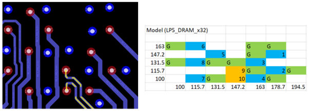
8.3.7.3. Example of an LPDDR5 Layout on an Altera® FPGA Platform Board
The following figures show the layout example of a single rank LPDDR5 x 32-bit device with a pitch size of 0.7×0.8mm on an Altera FPGA platform design.
The LPDDR5 signal routing is on upper layers to avoid vertical crosstalk on interface and achieve high performance.
Figure 69. Board Layout and Via Pattern for Single Rank LPDDR5 x32 device on an Altera FPGA Platform Design

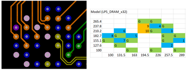
In addition, the following figure shows a LPDDR5 64-bit device board routing sample with pitch dimension of 0.4×0.4mm. The microvia has been used for via transitions on this interface. The microvia mentioned in the following is from top layer to layer 3, it belongs to Type-III stack-up for easier fan-out, not the same as microvia used in Type-IV stack-up. Only one lamination cycle is required, therefore the cost is not increased as much as microvias in Type-IV. You can also use normal PTH with backdrilling to fan out.
Figure 70. Board Via Pattern for LPDDR5 64-bit Device