External Memory Interfaces Agilex™ 7 M-Series FPGA IP User Guide
Visible to Intel only — GUID: bms1685486896583
Ixiasoft
- 4.1.2. s0_axi4_clock_out for Agilex 7 M-Series External Memory Interfaces (EMIF) IP - DDR4 Component
- 4.3.2. s0_axi4_clock_out for Agilex 7 M-Series External Memory Interfaces (EMIF) IP - DDR5 Component
Visible to Intel only — GUID: bms1685486896583
Ixiasoft
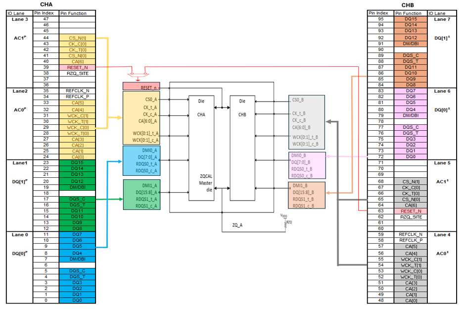
8.2.4.2. LPDDR5 Data Width Mapping
Only fixed byte lanes within the I/O bank can be used as data lanes. The following table lists the supported address and command and data lane placements in an I/O bank.
| Controller | Data Width Usage | BL7 [P95:P84] | BL6 [P83:P72] | BL5 [P71:P60] | BL4 [P59:P48] | BL3 [P47:P36] | BL2 [P35:P24] | BL1 [P23:P12] | BL0 [P11:P0] |
|---|---|---|---|---|---|---|---|---|---|
| Primary | LPDDR5 x16 | GPIO | GPIO | GPIO | GPIO | AC1 P | AC0 P | DQ[1] P | DQ[0] P |
| Primary 1 | LPDDR5 x16 | DQ[1] S | DQ[0] S | AC1 S | AC0 S | X | X | X | GPIO |
| Primary | LPDDR5 x32 | DQ[3] P | DQ[2] P | GPIO | GPIO | AC1 P | AC0 P | DQ[1] P | DQ[0] P |
|
Note:
|
|||||||||
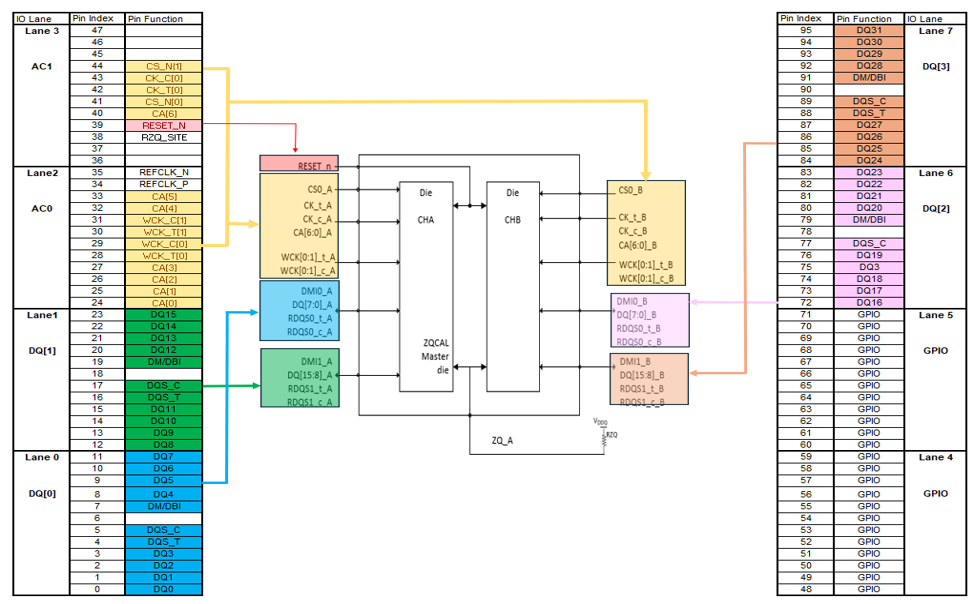
Refer to the Pin Options for LPDDR5 x32 figure in LPDDR5 Component Options for information on the T-line routing requirements for address and command pins.