Visible to Intel only — GUID: fqm1678993621623
Ixiasoft
1. FPGA AI Suite SoC Design Example User Guide
2. About the SoC Design Example
3. FPGA AI Suite SoC Design Example Quick Start Tutorial
4. FPGA AI Suite SoC Design Example Run Process
5. FPGA AI Suite SoC Design Example Build Process
6. FPGA AI Suite SoC Design Example Quartus® Prime System Architecture
7. FPGA AI Suite Soc Design Example Software Components
8. Streaming-to-Memory (S2M) Streaming Demonstration
A. FPGA AI Suite SoC Design Example User Guide Archives
B. FPGA AI Suite SoC Design Example User Guide Document Revision History
3.1. Initial Setup
3.2. Initializing a Work Directory
3.3. (Optional) Create an SD Card Image (.wic)
3.4. Writing the SD Card Image (.wic) to an SD Card
3.5. Preparing SoC FPGA Development Kits for the FPGA AI Suite SoC Design Example
3.6. Adding Compiled Graphs (AOT files) to the SD Card
3.7. Verifying FPGA Device Drivers
3.8. Running the Demonstration Applications
7.1.1. Yocto Recipe: recipes-core/images/coredla-image.bb
7.1.2. Yocto Recipe: recipes-bsp/u-boot/u-boot-socfpga_%.bbappend
7.1.3. Yocto Recipe: recipes-drivers/msgdma-userio/msgdma-userio.bb
7.1.4. Yocto Recipe: recipes-drivers/uio-devices/uio-devices.bb
7.1.5. Yocto Recipe: recipes-kernel/linux/linux-socfpga-lts_%.bbappend
7.1.6. Yocto Recipe: recipes-support/devmem2/devmem2_2.0.bb
7.1.7. Yocto Recipe: wic
Visible to Intel only — GUID: fqm1678993621623
Ixiasoft
6.5.2. The hps_0 Platform Designer Layer (hps.qys)
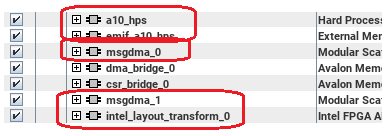
The hps_0 layer contains the HPS, an mSGDMA instance (msgdma_0) for the FPGA AI Suite runtime, and an mSGDMA instance (msgdma_1) for the streaming generation app (S2M variant only).
The example layout transform is also located here and can be replaced by your version.
