Visible to Intel only — GUID: czj1678993619388
Ixiasoft
1. FPGA AI Suite SoC Design Example User Guide
2. About the SoC Design Example
3. FPGA AI Suite SoC Design Example Quick Start Tutorial
4. FPGA AI Suite SoC Design Example Run Process
5. FPGA AI Suite SoC Design Example Build Process
6. FPGA AI Suite SoC Design Example Quartus® Prime System Architecture
7. FPGA AI Suite Soc Design Example Software Components
8. Streaming-to-Memory (S2M) Streaming Demonstration
A. FPGA AI Suite SoC Design Example User Guide Archives
B. FPGA AI Suite SoC Design Example User Guide Document Revision History
3.1. Initial Setup
3.2. Initializing a Work Directory
3.3. (Optional) Create an SD Card Image (.wic)
3.4. Writing the SD Card Image (.wic) to an SD Card
3.5. Preparing SoC FPGA Development Kits for the FPGA AI Suite SoC Design Example
3.6. Adding Compiled Graphs (AOT files) to the SD Card
3.7. Verifying FPGA Device Drivers
3.8. Running the Demonstration Applications
7.1.1. Yocto Recipe: recipes-core/images/coredla-image.bb
7.1.2. Yocto Recipe: recipes-bsp/u-boot/u-boot-socfpga_%.bbappend
7.1.3. Yocto Recipe: recipes-drivers/msgdma-userio/msgdma-userio.bb
7.1.4. Yocto Recipe: recipes-drivers/uio-devices/uio-devices.bb
7.1.5. Yocto Recipe: recipes-kernel/linux/linux-socfpga-lts_%.bbappend
7.1.6. Yocto Recipe: recipes-support/devmem2/devmem2_2.0.bb
7.1.7. Yocto Recipe: wic
Visible to Intel only — GUID: czj1678993619388
Ixiasoft
6.3.5.3. Layout Transform Configuration Options
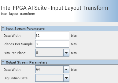
The example layout transform has a range of parameters to adjust to the data width based on the number of input planes being processed.
A maximum of 16 CSR mean and variance values are supported. The Planes per sample field sets this upper threshold.
All output data is in FP16 format which is the expected input format for the FPGA AI Suite.
