Visible to Intel only — GUID: dbs1602275463306
Ixiasoft
Visible to Intel only — GUID: dbs1602275463306
Ixiasoft
5.1. Top-Level Settings
| Parameter | Value | Default Value | Description |
|---|---|---|---|
| Hard IP Mode | Gen5 1x16, Interface - 1024-bit Gen4 1x16, Interface - 1024-bit Gen3 1x16, Interface - 1024-bit Gen4 1x16, Interface - 512-bit Gen3 1x16, Interface - 512-bit Gen5 2x8, Interface - 512-bit Gen4 2x8, Interface - 512-bit Gen3 2x8, Interface - 512-bit Gen4 2x8, Interface - 256-bit Gen3 2x8, Interface - 256-bit Gen5 4x4, Interface - 256-bit Gen4 4x4, Interface - 256-bit Gen3 4x4, Interface - 256-bit Gen4 4x4, Interface - 128-bit Gen3 4x4, Interface - 128-bit PIPE Direct 16-channel |
Gen5 1x16, Interface - 1024-bit |
Selects the width of the data interface between the transaction layer and the application layer implemented in the FPGA fabric, and the lane rate. Select the following elements:
Lane data rate:
Lane width:
Some of these configurations are only available in devices with the suffix R2 or R3 in their OPN number. For more details, refer to Avalon Streaming Interface Data and Header Bus Widths per Port. |
| Port Mode | Native Endpoint Root Port Downstream Upstream |
Native Endpoint |
Specifies the port type.
Note:
To operate the IP in TLP Bypass mode, choose either the Downstream or Upstream Port Mode. |
| PLD Clock Frequency | 500 MHz 475 MHz 450 MHz 425 MHz 400 MHz 300 MHz 275 MHz 250 MHz |
500 MHz (for Gen5 modes) 500 MHz / 300 MHz (for Gen4 and Gen3 modes, the default frequency depends on whether the IP is in double-width or single-width mode) |
Select the frequency of the Application clock. The options available vary depending on the setting of the Hard IP Mode parameter. For Gen5 modes, the available clock frequencies are 500 MHz / 475 MHz / 450 MHz / 425 MHz / 400 MHz. For Gen4 and Gen3 modes, the available clock frequencies depend on whether the IP is in double-width or single-width mode. For more details, refer to IP to FPGA Fabric Interface Summary. |
| Enable SRIS Mode | True/False | False | Enable the Separate Reference Clock with Independent Spread Spectrum Clocking (SRIS) feature. |
| Enable ASPM Control | No ASPM Support |
No ASPM Support L0s Supported L0s and L1 Supported L1 Supported |
Enables Active State Power Management (ASPM) Control in the Link Control register. |
| Enable CVP (INTEL VSEC) | True/False | False | When set, this parameter enables CVP for a single tile only. |
| Slow Clock Divider | 2 4 |
4 | Allows you to set the slow_clk to be divided by 2 or 4 from the coreclkout_hip. |
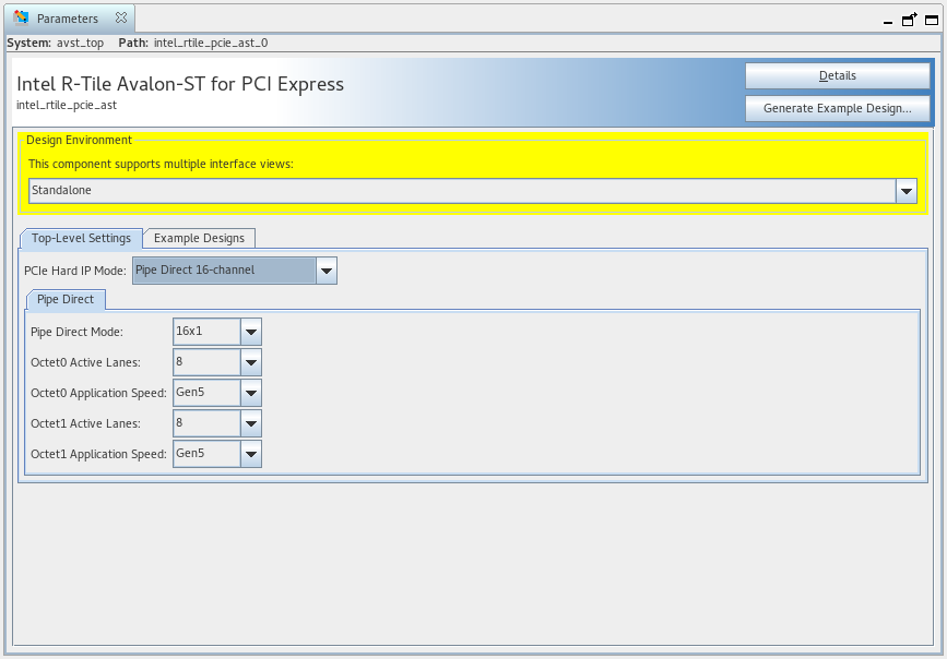
| PIPE Direct Mode | 1x16 2x8 4x4 8x2 2x4 / 1x8 4x2 / 1x8 8x1 / 1x8 1x8 / 2x4 4x2 / 2x4 8x1 / 2x4 1x8 / 4x2 2x4 / 4x2 8x1 / 4x2 1x8 / 8x1 2x4 / 8x1 4x2 / 8x1 16x1 |
16x1 | This option provides lane to lane TX deskew per grouping based on topologies. For example, if the 2x8 topology is selected, the EMIB is deskewed per every eight EMIB channels. This results in two sets of deskew markers, deskew errors, etc. |
| Octet 0 Active Lanes | Off 1 2 3 4 5 6 7 8 |
8 | Enables for lanes 0-7. This parameter indicates how many Lower lanes are used by the user application logic. |
| Octet 1 Active Lanes | Off 1 2 3 4 5 6 7 8 |
8 | Enables for lanes 8-15. This parameter indicates how many Upper lanes are used by the user application logic. |

