Visible to Intel only — GUID: GUID-E5296EC2-0E23-45A3-88CE-F68CD688EFEA
Visible to Intel only — GUID: GUID-E5296EC2-0E23-45A3-88CE-F68CD688EFEA
FPGA IP Authoring Flow
In the FPGA IP Authoring flow, the compiler uses your SYCL* code to generate IP components that you can integrate into a custom Intel® Quartus® Prime project. Use the IP authoring flow by targeting your compilation to a supported Intel® FPGA device family or part number instead of a specific acceleration platform.
Use this flow to help speed your IP development by letting you compile your SYCL* code to IP components on different targets that you can deploy into your systems.
For details about getting started with the IP component development flow, refer to Getting Started with Intel® oneAPI Toolkits and Intel® Quartus® Prime Software.
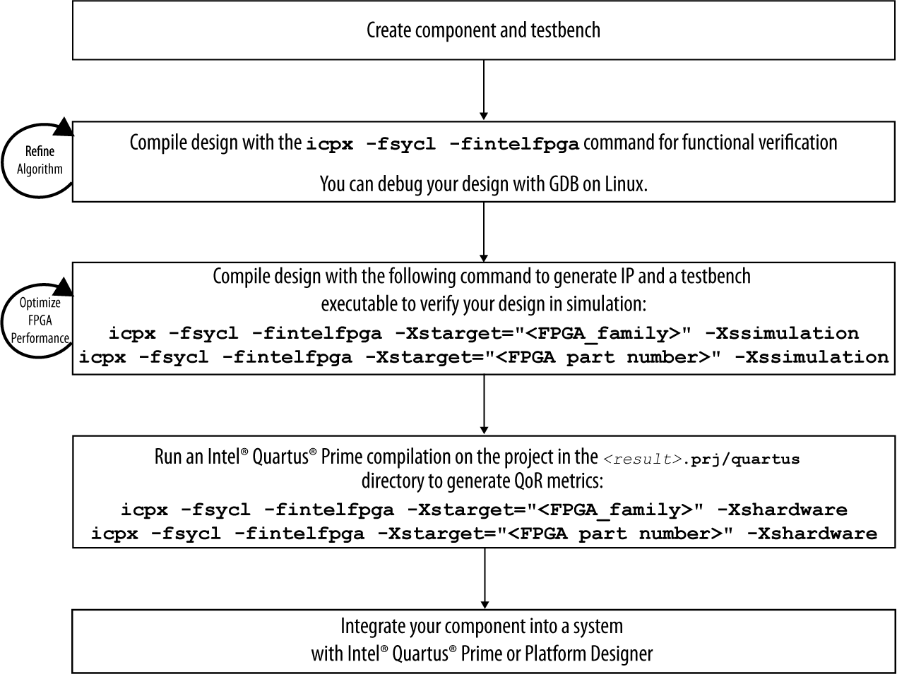
The typical design flow when you author IP components consists of the following stages:
Creating your IP component and testbench.
Write a complete SYCL application that contains both your IP component code and your testbench code. The SYCL device code (kernel code) corresponds to your IP component, and the SYCL host code serves as the testbench for the emulation and simulation flows.
For information about writing SYCL code, refer to Data Parallelism in C++ using SYCL*.
Also, refer to Code IP Components in SYCL* for additional information specific to writing IP components in SYCL*.
Verify the functionality of your IP component algorithm and testbench through emulation.
Verify the functionality of your IP component and refine the algorithms in your IP by compiling your design to an x86-64 executable and running the executable. For details, see Emulate and Debug Your IP Component.
Optimize and refine the FPGA performance of your component.
Optimize the FPGA performance of your component by compiling your design for an FPGA device family or part number target with the -Xstarget=<FPGA device family> or -Xstarget=<FPGA part number> compiler option along with -Xssimulation or -Xshardware option and reviewing the FPGA Optimization Report to see where you can optimize your component. This step generates RTL code for your component.
For details, refer to Analyze Your Design in the FPGA Optimization Guide for Intel® oneAPI Toolkits.
After completing some initial optimization based on the contents of the FPGA Optimization Report, you can see where to further refine your component by simulating it.
For details, see Evaluate Your IP Component Through Simulation.
Synthesize your component with an FPGA hardware image compilation.
When you use the -Xstarget=<FPGA device family> or -Xstarget=<FPGA part number> compiler option, the Intel® oneAPI DPC++/C++ Compiler ties the inputs and outputs of your component to virtual pins and compiles the design to provide a more accurate estimate of your component’s area and fMAX. The generated output is not deployable to a board because the compilation occurred without a board support package.
For details, refer to Synthesizing Your Component IP with Intel® Quartus® Prime Software.
Synthesizing your component generates accurate quality-of-results (QoR) metrics like FPGA area utilization and fMAX.
Integrate your IP into a system with Intel® Quartus® Prime or Platform Designer.
For details, refer to Integrating Your IP Into a System.
When you are satisfied with the predicted performance of your component, use Intel® Quartus® Prime software to synthesize your component. Synthesis also generates accurate area and performance (fMAX) estimates for your design. However, your design is not expected to cleanly close timing in the Intel® Quartus® Prime reports.
You can expect timing closure warnings in the Intel® Quartus® Prime logs because the generated project targets a clock speed of 1000 MHz to achieve the best possible placement for your design. The fMAX value presented in the FPGA optimization report estimates the maximum clock rate that your component can cleanly close timing for.
After the Intel® Quartus® Prime compilation is completed, the summary section of the FPGA optimization report shows the area and performance data for your components.
These estimates are more accurate than estimates generated when you compile your IP component for simulation only.
Typically, Intel® Quartus® Prime compilation times can take minutes to hours depending on the size and complexity of your IP components.
To synthesize your component IP and generate quality of results (QoR) data, instruct the compiler to run the Intel® Quartus® Prime compilation flow automatically after synthesizing the components. Include the -Xstarget=<FPGA device family> or -Xstarget=<FPGA part number> options in your icpx command:
icpx -fsycl -fintelfpga -Xshardware -Xstarget=<FPGA device family>...
icpx -fsycl -fintelfpga -Xshardware -Xstarget=<FPGA part number>...
The following flowchart shows a coarse-grained progression through the stages of a typical IP component authoring design flow.

- Code IP Components in SYCL*
- Emulate and Debug Your IP Component
- Evaluate Your IP Component Through Simulation
- FPGA IP Component Performance Optimization
- Synthesizing Your Component IP with Intel® Quartus® Prime Software
- Integrating Your IP Into a System
- Encrypt IP Components for Distribution