Visible to Intel only — GUID: qnr1727292066545
Ixiasoft
2.6. Compiling and Testing the Design
The GTS JESD204C Intel® FPGA IP parameter editor allows you to run the design example on a target development kit.
Perform the following steps to compile the design and program the development board:
- Launch the Quartus® Prime software and compile the design (Processing > Start Compilation). The timing constraints and pin assignments for the design example and the design components are automatically loaded during design example compilation.
- Connect the development board to the host computer either by connecting a USB cable to the on-board Intel® FPGA Download Cable II component or using an external Intel® FPGA Download Cable II module to connect to the external JTAG connector.
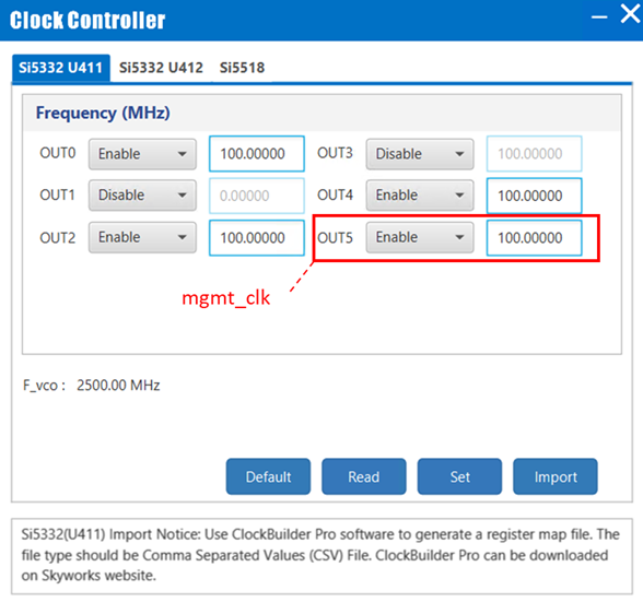
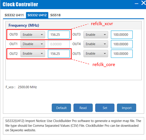
Table 7. Clock Settings Clock Name Clock Frequency refclk_xcvr Select the frequency for the transceiver PLL reference clock in the IP parameter editor. refclk_core Select the frequency for the core PLL reference clock in the IP parameter editor. mgmt_clk 100 MHz Figure 7. Clock Control GUI SettingsThe following example shows the clock control GUI settings for a design example running at 15.6025 Gbps.

- If you are performing external loopback test, attach the QSFP-DD loopback module at cage (U12).
- Configure the FPGA on the development board with the generated programming file (.sof file) using the Intel® Quartus® Prime Programmer.
To run the hardware testing using the Tcl script, refer to the Hardware Test for System Console Control Design Example section.