Visible to Intel only — GUID: ddz1678993619998
Ixiasoft
1. FPGA AI Suite SoC Design Example User Guide
2. About the SoC Design Example
3. FPGA AI Suite SoC Design Example Quick Start Tutorial
4. FPGA AI Suite SoC Design Example Run Process
5. FPGA AI Suite SoC Design Example Build Process
6. FPGA AI Suite SoC Design Example Quartus® Prime System Architecture
7. FPGA AI Suite Soc Design Example Software Components
8. Streaming-to-Memory (S2M) Streaming Demonstration
A. FPGA AI Suite SoC Design Example User Guide Archives
B. FPGA AI Suite SoC Design Example User Guide Document Revision History
3.1. Initial Setup
3.2. Initializing a Work Directory
3.3. (Optional) Create an SD Card Image (.wic)
3.4. Writing the SD Card Image (.wic) to an SD Card
3.5. Preparing SoC FPGA Development Kits for the FPGA AI Suite SoC Design Example
3.6. Adding Compiled Graphs (AOT files) to the SD Card
3.7. Verifying FPGA Device Drivers
3.8. Running the Demonstration Applications
7.1.1. Yocto Recipe: recipes-core/images/coredla-image.bb
7.1.2. Yocto Recipe: recipes-bsp/u-boot/u-boot-socfpga_%.bbappend
7.1.3. Yocto Recipe: recipes-drivers/msgdma-userio/msgdma-userio.bb
7.1.4. Yocto Recipe: recipes-drivers/uio-devices/uio-devices.bb
7.1.5. Yocto Recipe: recipes-kernel/linux/linux-socfpga-lts_5.15.bbappend
7.1.6. Yocto Recipe: wic
Visible to Intel only — GUID: ddz1678993619998
Ixiasoft
6.4. Top Level
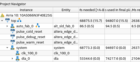
After the Quartus® Prime project has finished executing, the design should look similar to the following image in the Quartus® Prime Project Navigator:
Figure 10. SoC Design Example Hierarchy
The top-level Verilog file and HPS configuration is derived directly from the GSRD designs located at RocketBoards.org:
- For more information about the GSRD for the Agilex™ 7 FPGA I-Series Transceiver-SoC Development Kit, refer to the following URL https://www.rocketboards.org/foswiki/Documentation/AgilexSoCGSRDSIAGI027
- For more information about the GSRD for the Arria® 10 SX SoC FPGA Development Kit, refer to the following URL: https://www.rocketboards.org/foswiki/Documentation/arria10SoCGSRD
The GSRD designs have been modified to include the FPGA AI Suite IP. All unnecessary logic has been removed, which provides a concise design example.
The main FPGA AI Suite SoC design example is contained within a single Platform Designer system, called system. Double-click this node in the Quartus® Prime Project Navigator to launch Platform Designer.