Visible to Intel only — GUID: fod1719421391831
Ixiasoft
Visible to Intel only — GUID: fod1719421391831
Ixiasoft
2.7.2. Output Streaming
Use the output streaming component to stream output data from FPGA AI Suite IP to a downstream module using an AXI4-Stream interface.
When the output streaming interface enabled, it produces data in HWC format (where channels is the fastest changing dimension), on the output bus. The bus width is configured in the architecture parameters as described in Parameter Group: output_stream_interface. The data is converted from the FPGA AI Suite IP internal clock domain to the clock domain of the AXI4-Stream receiver.
| Signal | Source | Width | Description |
|---|---|---|---|
| clk_axi | Clock | 1 | Downstream AXI clock |
| i_resetn_axi | Reset | 1 | Downstream AXI active-low reset |
| o_ostream_axi_t_valid | FPGA AI Suite IP | 1 | Output signal that indicates whether the values in TDATA are valid |
| i_ostream_axi_t_ready | Downstream AXI User | 1 | Output signal that indicates whether the AXI receiver is ready to accept data |
| o_ostream_axi_t_data | FPGA AI Suite IP | DATA_WIDTH | Output data bus |
| o_ostream_axi_t_strb | FPGA AI Suite IP | DATA_WIDTH/8 | Output signal that indicates which bytes of TDATA are valid |
| o_ostream_axi_t_last | FPGA AI Suite IP | 1 | Indicates the last transmission for the current frame |
Data from the FPGA AI Suite IP is produced in CVEC multiples. When the number of output channels is not a multiple of CVEC, the last AXI4-Stream transaction for a single pixel in height/width dimensions might have only some valid elements that are indicated by the o_ostream_axi_t_strb signal.
Consider the following example: Assume the output data tensor has a shape of 3x3x10 (HWC), with CVEC = 8 elements (each 16 bits), and AXI TDATA_WIDTH = 128 bits. For each pixel in the 3x3 surface, we need to produce 10 channels, which fit in two AXI transactions. The first transaction has all valid elements (o_ostream_axi_t_strb = 0xffff). The second transaction has only two valid elements and the rest are zeros (o_ostream_axi_t_strb = 0x000f). The downstream receiver of AXI transactions is responsible for intercepting the o_ostream_axi_t_strb signal and processing only the valid elements.
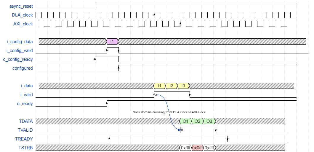
The figure that follows demonstrates an example transaction flow with 3 input transactions (I1, I2 and I3, each 128 bits) and three output AXI transactions (O1, O2, and O3, each 128 bits). In this example the first and third 128-bit transactions are all valid data (o_ostream_axi_t_strb =0xffff), but the second transaction has only 6 valid elements (16 valid bytes). For the second transaction, the o_ostream_axi_t_strb =0x0fff (marked in red color). Notice that data transactions happen only when the block is configured and ready to produce output.
