Visible to Intel only — GUID: mwh1410471086403
Ixiasoft
Visible to Intel only — GUID: mwh1410471086403
Ixiasoft
1.7.3. Defining PCB Layers and PCB Layer Thickness
You can specify the number of layers on you PCB, and their thickness. The PCB layer information is used only during SSN analysis and is not used in other processes run by the Intel® Quartus® Prime software. If a custom PCB breakout region is not described you can select the default thickness, which directs the SSN Analyzer to use a single-layer PCB breakout region during SSN analysis.
All the assignments you create for the PCB layers are saved to the .qsf. You can also use Tcl commands to create PCB layer assignments. You can create any number of PCB layers, however, the layers must be consecutive.
Tcl Commands for Specifying PCB Layer Assignments
set_global_assignment -name PCB_LAYER_THICKNESS 0.00099822M -section_id 1 set_global_assignment -name PCB_LAYER_THICKNESS 0.00034036M -section_id 2 set_global_assignment -name PCB_LAYER_THICKNESS 0.00034036M -section_id 3
The cross-section shows the stackup information of a PCB, which tells you the number of layers used in your PCB. The PCB shown in this example consists of various signal and circuit layers on which FPGA pins are routed, as well as the power and ground layers.

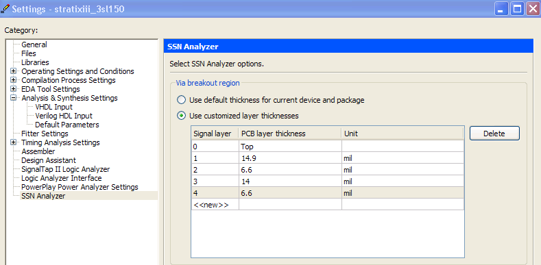
In this example, each of the four signal layers are a different thickness, with the depths shown in the Thickness (MIL) column. The layer thickness for each signal layer is computed as follows:
- Signal Layer 1 is the L4-SIGNAL, at thickness (1.9+3.6+1.2+3+1.2+4=) 14.9 mils
- Signal Layer 2 is the L5-SIGNAL, at thickness (0.6+6=) 6.6 mils
- Signal Layer 3 is the L8-SIGNAL, at thickness (0.6+4+1.2+3+1.2+4=) 14 mils
- Signal Layer 4 is the L9-SIGNAL, at thickness (0.6+6=) 6.6 mils
Figure 10. PCB Layers and Thickness Assignments Specified in the Intel® Quartus® Prime Software
