Visible to Intel only — GUID: rlz1592875069184
Ixiasoft
Visible to Intel only — GUID: rlz1592875069184
Ixiasoft
3.3.1. Testbench Overview

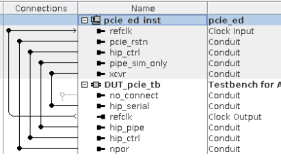
The testbench uses a Root Port driver module to initiate the configuration and exercise the target memory and DMA channel in the Endpoint. This is the module that you can modify to vary the transactions sent to the example Endpoint design or your own design.
- MCDMA P-Tile testbench
Path: pcie_ed_tb/ip/pcie_ed_tb/DUT_pcie_tb_ip/intel_pcie_ptile_tbed_100/sim
File: altpcietb_bfm_rp_gen4_x16.sv
- MCDMA F-Tile testbench
Path: pcie_ed_tb/ip/pcie_ed_tb/dut_pcie_tb_ip/intel_pcie_ftile_tbed_100/sim
File: altpcietb_bfm_rp_gen4_x16.sv
- MCDMA H-Tile testbench
Path: pcie_ed_tb/ip/pcie_ed_tb/DUT_pcie_tb_ip/altera_pcie_s10_tbed_191/sim
File: altpcietb_bfm_rp_gen3_x8.sv