Visible to Intel only — GUID: nik1412379636551
Ixiasoft
Visible to Intel only — GUID: nik1412379636551
Ixiasoft
3.1. Methodology
This simulation emulates an Intel Stratix® V GX transmitter (with embedded package model), a PCI Express* 8GT receiver (with embedded package model), and a ~18-inch backplane channel. Per PCI Express* 8GT specifications, the link operates at 8 Gbps with a bit error rate (BER) < 10–12. The transmitter must have a minimum differential output voltage of 800 mV and a rise/fall time of ~35 ps (at 0.8 V VOD). In this simulation, the Stratix® V GX transmitter is set to 800 mV VOD (VOD level = 40). Additionally, the Stratix® V GX transmitter has a 4-tap FIR to compensate for channel effects. The PCI Express* 8G receiver has CTLE and a 1-Tap DFE per PCI-SIG definition.
To accomplish these goals, set up a transmitter model, a receiver model, and a link with the following parameters:
- Data rate: 8 Gbps
- Test pattern: PRBS-23
- BER target: BER < 10–12
- Stratix® V GX transmitter
- VOD: 800 mV (VOD Level = 40)
- Edge rate: Per Stratix® V GX characteristics
- 4-Tap TX FIR (1 pre-tap and 2 post-taps)
- Stratix® V GX package model (embedded)
- PLL: ATX (LC) set to low bandwidth
- Output Jitter: Retrieved from the Intel Characterization Database (embedded in Intel® Advanced Link Analyzer; contact My Intel support to enable this function)
- DCD = ~0.012 UI
- BUJ = ~0.032 UI
- RJ = ~1.00 psRMS (8 Gbps, BER < 10–12)
- Receiver
- CTLE:
- Programmable with 6 dB~12 dB boost at 4 GHz
- Per PCI-SIG specifications
- 1-tap DFE
- PCI-SIG receiver package model (12-port S-parameter model from PCI-SIG)
- CDR: Generic binary CDR with high loop bandwidth ~26 MHz
- Receiver Jitter:
- DJ = ~7 ps
- RJ = ~1.55 psRMS (at BER < 10–12)
- CTLE:
The ~18-inch backplane channel is described by a 12-port S-parameter model. The S-parameter is measured (or generated) with port configuration type 2, as shown in the following figure:


The Intel® Advanced Link Analyzer Channel Viewer shows that the backplane channel has approximately 17.15 dB loss at 4 GHz. The PCI-SIG RX package has 3.5 dB insertion loss at 4 GHz. The overall link has about 21 dB of loss (as shown in the Combined Channel black curve, not including Stratix® V GX transmitter package) at 4 GHz, which requires heavy TX and RX equalizations to achieve the required BER target.
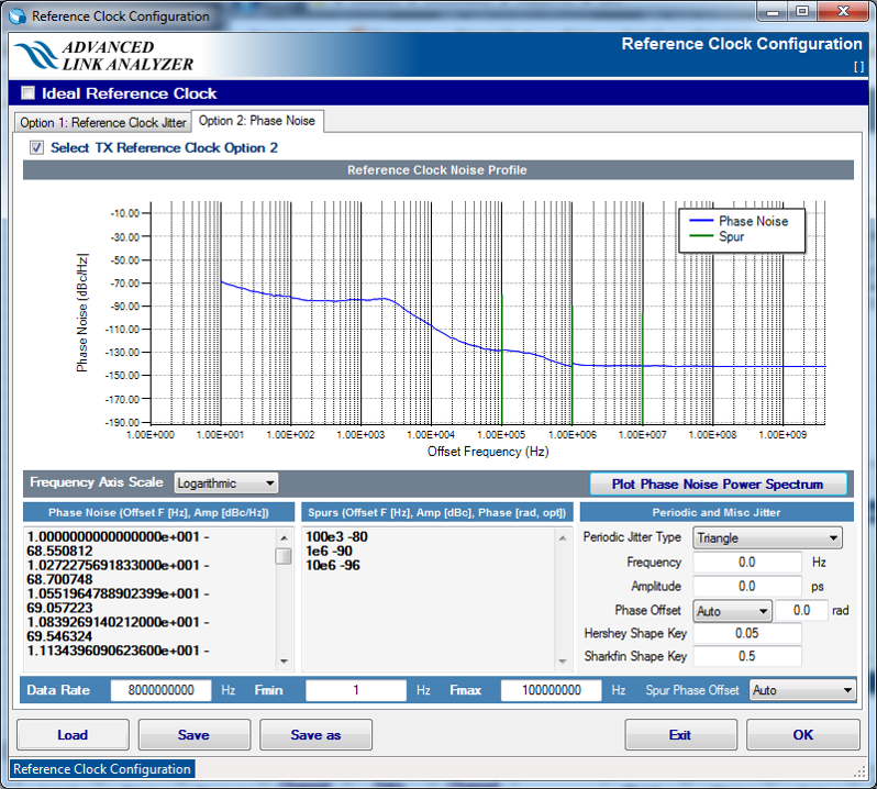
For comparative purposes, the following table and figure show a typical external 100 MHz transmitter reference clock with measured phase noise characteristics and spurs at three different frequencies.
| Phase Noise |
Spurs |
||
|---|---|---|---|
| Frequency |
Phase Noise (dBc) |
Frequency |
Amplitude (dBc) |
| 10 Hz |
–68 |
100 kHz |
–80 |
| 100 Hz |
–82 |
1 MHz |
–90 |
| 1 kHz |
–84 |
10 MHz |
–96 |
| 1 MHz and above |
–140 |
||

The PLL in the Stratix® V GX transmitter is enabled using ATX (LC) with low bandwidth configuration. The PLL effectively reduces the noise effects from the external reference clock.
Use the Intel® Advanced Link Analyzer’s link optimization algorithm to find the optimal equalization settings for both the transmitter and receiver. In this demonstration, you use the CTLE=>FIR+DFE link optimization method.