Visible to Intel only — GUID: mwh1409960096878
Ixiasoft
1. Design Optimization Overview
2. Optimizing the Design Netlist
3. Timing Closure and Optimization
4. Area Optimization
5. Analyzing and Optimizing the Design Floorplan
6. Netlist Optimizations and Physical Synthesis
7. Engineering Change Orders with the Chip Planner
A. Intel® Quartus® Prime Standard Edition User Guides
2.1. When to Use the Netlist Viewers: Analyzing Design Problems
2.2. Intel® Quartus® Prime Design Flow with the Netlist Viewers
2.3. RTL Viewer Overview
2.4. State Machine Viewer Overview
2.5. Technology Map Viewer Overview
2.6. Netlist Viewer User Interface
2.7. Schematic View
2.8. State Machine Viewer
2.9. Cross-Probing to a Source Design File and Other Intel® Quartus® Prime Windows
2.10. Cross-Probing to the Netlist Viewers from Other Intel® Quartus® Prime Windows
2.11. Viewing a Timing Path
2.12. Optimizing the Design Netlist Revision History
2.7.1. Display Schematics in Multiple Tabbed View
2.7.2. Schematic Symbols
2.7.3. Select Items in the Schematic View
2.7.4. Shortcut Menu Commands in the Schematic View
2.7.5. Filtering in the Schematic View
2.7.6. View Contents of Nodes in the Schematic View
2.7.7. Moving Nodes in the Schematic View
2.7.8. View LUT Representations in the Technology Map Viewer
2.7.9. Zoom Controls
2.7.10. Navigating with the Bird's Eye View
2.7.11. Partition the Schematic into Pages
2.7.12. Follow Nets Across Schematic Pages
3.1. Optimize Multi Corner Timing
3.2. Critical Paths
3.3. Design Evaluation for Timing Closure
3.4. Design Analysis
3.5. Timing Optimization
3.6. Periphery to Core Register Placement and Routing Optimization
3.77.7. Scripting Support3.77.7. Scripting Support
3.8. Timing Closure and Optimization Revision History
3.4.3.1. Displaying Path Reports with the Timing Analyzer
3.4.3.2. Tips for Analyzing Failing Paths
3.4.3.3. Tips for Analyzing Failing Clock Paths that Cross Clock Domains
3.4.3.4. Tips for Analyzing Paths from/to the Source and Destination of Critical Path
3.4.3.5. Tips for Creating a .tcl Script to Monitor Critical Paths Across Compiles
3.4.3.6. Global Routing Resources
3.5.1. Displaying Timing Closure Recommendations for Failing Paths
3.5.2. Timing Optimization Advisor
3.5.3. Optional Fitter Settings
3.5.4. I/O Timing Optimization Techniques
3.5.5. Register-to-Register Timing Optimization Techniques
3.5.6. Logic Lock (Standard) Assignments
3.5.7. Location Assignments
3.5.8. Metastability Analysis and Optimization Techniques
3.5.4.1. Optimize IOC Register Placement for Timing Logic Option
3.5.4.2. Fast Input, Output, and Output Enable Registers
3.5.4.3. Programmable Delays
3.5.4.4. Use PLLs to Shift Clock Edges
3.5.4.5. Use Fast Regional Clock Networks and Regional Clocks Networks
3.5.4.6. Spine Clock Limitations
3.5.4.7. Change How Hold Times are Optimized for Devices
3.5.5.1. Optimize Source Code
3.5.5.2. Improving Register-to-Register Timing
3.5.5.3. Physical Synthesis Optimizations
3.5.5.4. Turn Off Extra-Effort Power Optimization Settings
3.5.5.5. Optimize Synthesis for Speed, Not Area
3.5.5.6. Flatten the Hierarchy During Synthesis
3.5.5.7. Set the Synthesis Effort to High
3.5.5.8. Change State Machine Encoding
3.5.5.9. Duplicate Logic for Fan-Out Control
3.5.5.10. Prevent Shift Register Inference
3.5.5.11. Use Other Synthesis Options Available in Your Synthesis Tool
3.5.5.12. Fitter Seed
3.5.5.13. Set Maximum Router Timing Optimization Level
4.2.4.1. Guideline: Optimize Source Code
4.2.4.2. Guideline: Optimize Synthesis for Area, Not Speed
4.2.4.3. Guideline: Restructure Multiplexers
4.2.4.4. Guideline: Perform WYSIWYG Primitive Resynthesis with Balanced or Area Setting
4.2.4.5. Guideline: Use Register Packing
4.2.4.6. Guideline: Remove Fitter Constraints
4.2.4.7. Guideline: Flatten the Hierarchy During Synthesis
4.2.4.8. Guideline: Re-target Memory Blocks
4.2.4.9. Guideline: Use Physical Synthesis Options to Reduce Area
4.2.4.10. Guideline: Retarget or Balance DSP Blocks
4.2.4.11. Guideline: Use a Larger Device
4.2.5.1. Guideline: Set Auto Packed Registers to Sparse or Sparse Auto
4.2.5.2. Guideline: Set Fitter Aggressive Routability Optimizations to Always
4.2.5.3. Guideline: Increase Router Effort Multiplier
4.2.5.4. Guideline: Remove Fitter Constraints
4.2.5.5. Guideline: Optimize Synthesis for Area, Not Speed
4.2.5.6. Guideline: Optimize Source Code
4.2.5.7. Guideline: Use a Larger Device
5.1.1. Starting the Chip Planner
5.1.2. Chip Planner GUI Components
5.1.3. Viewing Architecture-Specific Design Information
5.1.4. Viewing Available Clock Networks in the Device
5.1.5. Viewing Routing Congestion
5.1.6. Viewing I/O Banks
5.1.7. Viewing High-Speed Serial Interfaces (HSSI)
5.1.8. Viewing the Source and Destination of Placed Nodes
5.1.9. Viewing Fan-In and Fan-Out Connections of Placed Resources
5.1.10. Generating Immediate Fan-In and Fan-Out Connections
5.1.11. Exploring Paths in the Chip Planner
5.1.12. Viewing Assignments in the Chip Planner
5.1.13. Viewing High-Speed and Low-Power Tiles in the Chip Planner
5.1.14. Viewing Design Partition Placement
5.2.1. Attributes of a Logic Lock (Standard) Region
5.2.2. Creating Logic Lock (Standard) Regions
5.2.3. Customizing the Shape of Logic Lock Regions
5.2.4. Placing Logic Lock (Standard) Regions
5.2.5. Placing Device Resources into Logic Lock (Standard) Regions
5.2.6. Hierarchical (Parent and Child) Logic Lock (Standard) Regions
5.2.7. Additional Intel® Quartus® Prime Logic Lock (Standard) Design Features
5.2.8. Logic Lock (Standard) Regions Window
5.2.2.1. Creating Logic Lock (Standard) Regions with the Chip Planner
5.2.2.2. Creating Logic Lock (Standard) Regions with the Project Navigator
5.2.2.3. Creating Logic Lock (Standard) Regions with the Logic Lock (Standard) Regions Window
5.2.2.4. Defining Routing Regions
5.2.2.5. Noncontiguous Logic Lock (Standard) Regions
5.2.2.6. Considerations on Using Auto Sized Regions
5.4.1. Initializing and Uninitializing a Logic Lock (Standard) Region
5.4.2. Creating or Modifying Logic Lock (Standard) Regions
5.4.3. Obtaining Logic Lock (Standard) Region Properties
5.4.4. Assigning Logic Lock (Standard) Region Content
5.4.5. Save a Node-Level Netlist for the Entire Design into a Persistent Source File
5.4.6. Setting Logic Lock (Standard) Assignment Priority
5.4.7. Assigning Virtual Pins with a Tcl command
7.1. Engineering Change Orders
7.2. ECO Design Flow
7.3. The Chip Planner Overview
7.4. Performing ECOs with the Chip Planner (Floorplan View)
7.5. Performing ECOs in the Resource Property Editor
7.6. Change Manager
3.77.7. Scripting Support3.77.7. Scripting Support
7.8. Common ECO Applications
7.9. Post ECO Steps
7.10. Engineering Change Orders with the Chip Planner Revision History
Visible to Intel only — GUID: mwh1409960096878
Ixiasoft
2.6. Netlist Viewer User Interface
The Netlist Viewer is a graphical user-interface for viewing and manipulating nodes and nets in the netlist.
The RTL Viewer and Technology Map Viewer each consist of these main parts:
- The Netlist Navigator pane—displays a representation of the project hierarchy.
- The Find pane—allows you to find and locate specific design elements in the schematic view.
- The Properties pane displays the properties of the selected block when you select Properties from the shortcut menu.
- The schematic view—displays a graphical representation of the internal structure of the design.
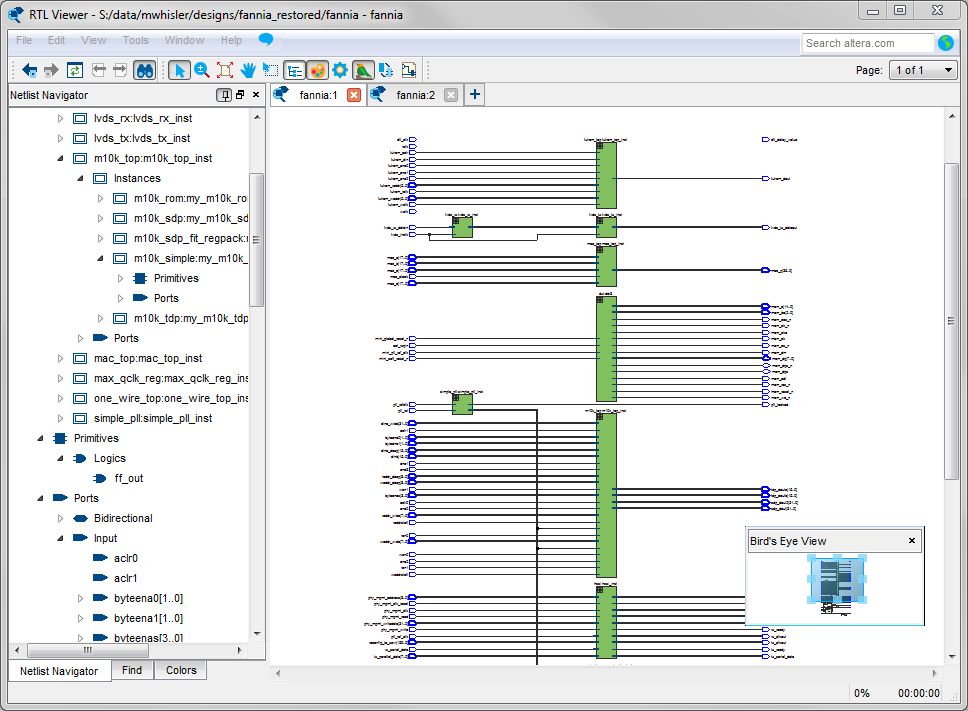
Figure 3. RTL Viewer
Netlist Viewers also contain a toolbar that provides tools to use in the schematic view.
- Use the Back and Forward buttons to switch between schematic views. You can go forward only if you have not made any changes to the view since going back. These commands do not undo an action, such as selecting a node. The Netlist Viewer caches up to ten actions including filtering, hierarchy navigation, netlist navigation, and zoom actions.
- The Refresh button to restore the schematic view and optimizes the layout. Refresh does not reload the database if you change the design and recompile.
- Click the Find button opens and closes the Find pane.
- Click the Selection Tool and Zoom Tool buttons to alternate between the selection mode and zoom mode.
- Click the Fit in Page button resets the schematic view to encompass the entire design.
- Use the Hand Tool to change the focus of the viewer without changing the perspective.
- Click the Area Selection Tool to drag a selection box around ports, pins, and nodes in an area.
- Click the Netlist Navigator button to open or close the Netlist Navigator pane.
- Click the Color Settings button to open the Colors pane where you can customize the Netlist Viewer color scheme.
- Click the Display Settings button to open the Display pane where you can specify the following settings:
- Show full name or Show only <n> characters. You can specify this separately for Node name, Port name, Pin name, or Bus name.
- Turn Show timing info on or off.
- Turn Show node type on or off.
- Turn Show constant value on or off.
- Turn Show flat nets on or off.
Figure 4. Display Settings - The Bird's Eye View button opens the Bird's Eye View window which displays a miniature version of the design and allows you to navigate within the design and adjust the magnification in the schematic view quickly.
- The Show/Hide Instance Pins button can alternate the display of instance pins not displayed by functions such as cross-probing between a Netlist Viewer and Timing Analyzer. You can also use this button to hide unconnected instance pins when filtering a node results in large numbers of unconnected or unused pins. The Netlist Viewer hides Instance pins by default.
- If the Netlist Viewer display encompasses several pages, the Show Netlist on One Page button resizes the netlist view to a single page. This action can make netlist tracing easier.
You can have only one RTL Viewer, one Technology Map Viewer (Post-Fitting), one Technology Map Viewer (Post-Mapping), and one State Machine Viewer window open at the same time, although each window can show multiple pages, each with multiple tabs. For example, you cannot have two RTL Viewer windows open at the same time.