Intel® Quartus® Prime Standard Edition User Guide: Design Optimization
ID
683230
Date
11/12/2018
Public
1. Design Optimization Overview
2. Optimizing the Design Netlist
3. Timing Closure and Optimization
4. Area Optimization
5. Analyzing and Optimizing the Design Floorplan
6. Netlist Optimizations and Physical Synthesis
7. Engineering Change Orders with the Chip Planner
A. Intel® Quartus® Prime Standard Edition User Guides
2.1. When to Use the Netlist Viewers: Analyzing Design Problems
2.2. Intel® Quartus® Prime Design Flow with the Netlist Viewers
2.3. RTL Viewer Overview
2.4. State Machine Viewer Overview
2.5. Technology Map Viewer Overview
2.6. Netlist Viewer User Interface
2.7. Schematic View
2.8. State Machine Viewer
2.9. Cross-Probing to a Source Design File and Other Intel® Quartus® Prime Windows
2.10. Cross-Probing to the Netlist Viewers from Other Intel® Quartus® Prime Windows
2.11. Viewing a Timing Path
2.12. Optimizing the Design Netlist Revision History
2.7.1. Display Schematics in Multiple Tabbed View
2.7.2. Schematic Symbols
2.7.3. Select Items in the Schematic View
2.7.4. Shortcut Menu Commands in the Schematic View
2.7.5. Filtering in the Schematic View
2.7.6. View Contents of Nodes in the Schematic View
2.7.7. Moving Nodes in the Schematic View
2.7.8. View LUT Representations in the Technology Map Viewer
2.7.9. Zoom Controls
2.7.10. Navigating with the Bird's Eye View
2.7.11. Partition the Schematic into Pages
2.7.12. Follow Nets Across Schematic Pages
3.1. Optimize Multi Corner Timing
3.2. Critical Paths
3.3. Design Evaluation for Timing Closure
3.4. Design Analysis
3.5. Timing Optimization
3.6. Periphery to Core Register Placement and Routing Optimization
3.77.7. Scripting Support3.77.7. Scripting Support
3.8. Timing Closure and Optimization Revision History
3.4.3.1. Displaying Path Reports with the Timing Analyzer
3.4.3.2. Tips for Analyzing Failing Paths
3.4.3.3. Tips for Analyzing Failing Clock Paths that Cross Clock Domains
3.4.3.4. Tips for Analyzing Paths from/to the Source and Destination of Critical Path
3.4.3.5. Tips for Creating a .tcl Script to Monitor Critical Paths Across Compiles
3.4.3.6. Global Routing Resources
3.5.1. Displaying Timing Closure Recommendations for Failing Paths
3.5.2. Timing Optimization Advisor
3.5.3. Optional Fitter Settings
3.5.4. I/O Timing Optimization Techniques
3.5.5. Register-to-Register Timing Optimization Techniques
3.5.6. Logic Lock (Standard) Assignments
3.5.7. Location Assignments
3.5.8. Metastability Analysis and Optimization Techniques
3.5.4.1. Optimize IOC Register Placement for Timing Logic Option
3.5.4.2. Fast Input, Output, and Output Enable Registers
3.5.4.3. Programmable Delays
3.5.4.4. Use PLLs to Shift Clock Edges
3.5.4.5. Use Fast Regional Clock Networks and Regional Clocks Networks
3.5.4.6. Spine Clock Limitations
3.5.4.7. Change How Hold Times are Optimized for Devices
3.5.5.1. Optimize Source Code
3.5.5.2. Improving Register-to-Register Timing
3.5.5.3. Physical Synthesis Optimizations
3.5.5.4. Turn Off Extra-Effort Power Optimization Settings
3.5.5.5. Optimize Synthesis for Speed, Not Area
3.5.5.6. Flatten the Hierarchy During Synthesis
3.5.5.7. Set the Synthesis Effort to High
3.5.5.8. Change State Machine Encoding
3.5.5.9. Duplicate Logic for Fan-Out Control
3.5.5.10. Prevent Shift Register Inference
3.5.5.11. Use Other Synthesis Options Available in Your Synthesis Tool
3.5.5.12. Fitter Seed
3.5.5.13. Set Maximum Router Timing Optimization Level
4.2.4.1. Guideline: Optimize Source Code
4.2.4.2. Guideline: Optimize Synthesis for Area, Not Speed
4.2.4.3. Guideline: Restructure Multiplexers
4.2.4.4. Guideline: Perform WYSIWYG Primitive Resynthesis with Balanced or Area Setting
4.2.4.5. Guideline: Use Register Packing
4.2.4.6. Guideline: Remove Fitter Constraints
4.2.4.7. Guideline: Flatten the Hierarchy During Synthesis
4.2.4.8. Guideline: Re-target Memory Blocks
4.2.4.9. Guideline: Use Physical Synthesis Options to Reduce Area
4.2.4.10. Guideline: Retarget or Balance DSP Blocks
4.2.4.11. Guideline: Use a Larger Device
4.2.5.1. Guideline: Set Auto Packed Registers to Sparse or Sparse Auto
4.2.5.2. Guideline: Set Fitter Aggressive Routability Optimizations to Always
4.2.5.3. Guideline: Increase Router Effort Multiplier
4.2.5.4. Guideline: Remove Fitter Constraints
4.2.5.5. Guideline: Optimize Synthesis for Area, Not Speed
4.2.5.6. Guideline: Optimize Source Code
4.2.5.7. Guideline: Use a Larger Device
5.1.1. Starting the Chip Planner
5.1.2. Chip Planner GUI Components
5.1.3. Viewing Architecture-Specific Design Information
5.1.4. Viewing Available Clock Networks in the Device
5.1.5. Viewing Routing Congestion
5.1.6. Viewing I/O Banks
5.1.7. Viewing High-Speed Serial Interfaces (HSSI)
5.1.8. Viewing the Source and Destination of Placed Nodes
5.1.9. Viewing Fan-In and Fan-Out Connections of Placed Resources
5.1.10. Generating Immediate Fan-In and Fan-Out Connections
5.1.11. Exploring Paths in the Chip Planner
5.1.12. Viewing Assignments in the Chip Planner
5.1.13. Viewing High-Speed and Low-Power Tiles in the Chip Planner
5.1.14. Viewing Design Partition Placement
5.2.1. Attributes of a Logic Lock (Standard) Region
5.2.2. Creating Logic Lock (Standard) Regions
5.2.3. Customizing the Shape of Logic Lock Regions
5.2.4. Placing Logic Lock (Standard) Regions
5.2.5. Placing Device Resources into Logic Lock (Standard) Regions
5.2.6. Hierarchical (Parent and Child) Logic Lock (Standard) Regions
5.2.7. Additional Intel® Quartus® Prime Logic Lock (Standard) Design Features
5.2.8. Logic Lock (Standard) Regions Window
5.2.2.1. Creating Logic Lock (Standard) Regions with the Chip Planner
5.2.2.2. Creating Logic Lock (Standard) Regions with the Project Navigator
5.2.2.3. Creating Logic Lock (Standard) Regions with the Logic Lock (Standard) Regions Window
5.2.2.4. Defining Routing Regions
5.2.2.5. Noncontiguous Logic Lock (Standard) Regions
5.2.2.6. Considerations on Using Auto Sized Regions
5.4.1. Initializing and Uninitializing a Logic Lock (Standard) Region
5.4.2. Creating or Modifying Logic Lock (Standard) Regions
5.4.3. Obtaining Logic Lock (Standard) Region Properties
5.4.4. Assigning Logic Lock (Standard) Region Content
5.4.5. Save a Node-Level Netlist for the Entire Design into a Persistent Source File
5.4.6. Setting Logic Lock (Standard) Assignment Priority
5.4.7. Assigning Virtual Pins with a Tcl command
7.1. Engineering Change Orders
7.2. ECO Design Flow
7.3. The Chip Planner Overview
7.4. Performing ECOs with the Chip Planner (Floorplan View)
7.5. Performing ECOs in the Resource Property Editor
7.6. Change Manager
3.77.7. Scripting Support3.77.7. Scripting Support
7.8. Common ECO Applications
7.9. Post ECO Steps
7.10. Engineering Change Orders with the Chip Planner Revision History
7.5.3.4. Cyclone V I/O Elements
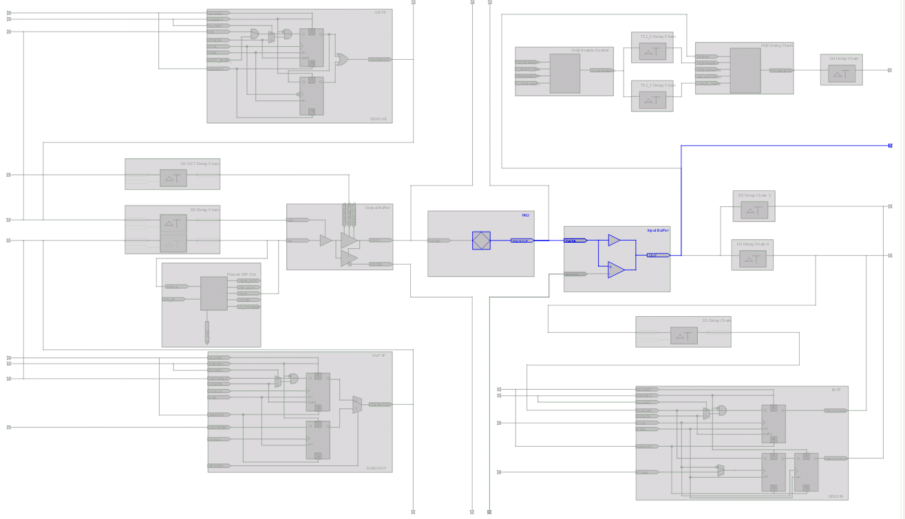
The I/O elements in Cyclone V devices contain a bidirectional I/O buffer and registers for complete embedded bidirectional single data rate transfer. The I/O element contains three input register, two output registers, and two output-enable registers. The two output registers and two output-enable registers are utilized for double-data rate (DDR) applications.
You can use the input registers for fast setup times and the output registers for fast clock-to-output times. Additionally, you can use the output-enable (OE) registers for fast clock-to-output enable timing. You can use I/O elements for input, output, or bidirectional data paths. By default, the Intel® Quartus® Prime software displays the used resources in blue and the unused resources in gray.
Figure 56. Cyclone V Device I/O Elements and Structure

