1.3. Functional Description for the Single Root I/O Virtualization (SR-IOV) Design Example
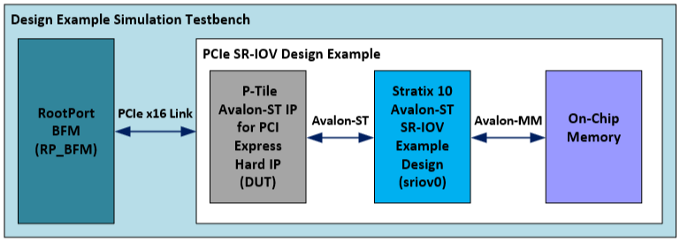
The SR-IOV design example performs memory transfers from a host processor to a target device. It supports up to two PFs and 32 VFs per PF.
The SR-IOV design example automatically creates the files necessary to simulate and compile in the Intel® Quartus® Prime software. You can download the compiled design to an Intel® Stratix® 10 DX Development Kit or an Intel® Agilex™ Development Kit.
This design example includes the following components:
- The generated P-Tile Avalon Streaming (Avalon-ST) IP Endpoint variant (DUT) with the parameters you specified. This component drives the received TLP data to the SR-IOV application.
- The SR-IOV Application (APPS) component, which performs the necessary translation between the PCI Express TLPs and simple Avalon-ST writes and reads to the on-chip memory. For the SR-IOV APPS component, a memory read TLP generates a Completion with data.
- For an SR-IOV design example with two PFs and 32 VFs per PF, there are 66 memory locations that the design example can access. The two PFs can access two memory locations, while the 64 VFs (2 x 32) can access 64 memory locations.
- A Reset Release IP.
The simulation testbench instantiates the SR-IOV design example and a Root Port BFM to interface with the target Endpoint.


The test program writes to and reads back data from the same location in the on-chip memory across 2 PFs and 32 VFs per PF. It compares the data read to the expected result. The test reports, "Simulation stopped due to successful completion" if no errors occur.
The SR-IOV design example supports the following configurations:
- Gen4 x16 512-bit (350 MHz or above) Endpoint
- Gen3 x16 512-bit Endpoint
- Gen4 x8x8 256-bit (350 MHz or above) Endpoint
- Gen3 x8x8 256-bit Endpoint

