6.1.5. D-PHY TX PPI Interface Signals
These PPI interface signals are available when the D-PHY IP is configured for transmit. Each lane (clock and data) of each link has a TX PPI interface attached to it.
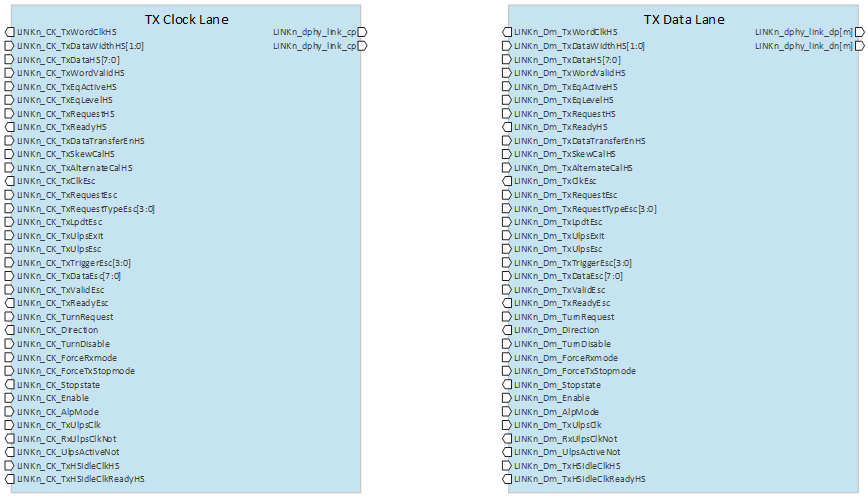
Figure 24. PPI Interface Signals (Clock and Data Lanes)
| Signal | Direction | Width | Description |
|---|---|---|---|
| High-Speed Transmit Signals (Link n, Clock Lane) - TX only | |||
| LINKn_CK_TxWordClkHS | Output | 1 | High-Speed Transmit Word Clock (link n, clock lane) This is used to synchronize PPI signals in the high-speed transmit clock domain. It is recommended that all transmitting Lane Modules share one TxWordClkHS signal. The frequency of TxWordClkHS is dependent upon the width of the High-Speed Transmit Data, as follows: • 16-bit width, TxDataHS[15:0], the High-Speed Transmit Word Clock is exactly 1/16 the high-speed data rate. |
| LINKn_CK_TxDataWidthHS | Input | 2 | High-Speed Transmit Data bus Width Select (link n, clock lane). |
| LINKn_CK_TxDataHS | Input | 8 | High-Speed Transmit Data bus (link n, clock lane). |
| LINKn_CK_TxWordValidHS | Input | 1 | High-Speed Transmit Word Data Valid (link n, clock lane) When the High-Speed Transmit Data width is greater than 8 bits it is necessary to indicate which 8-bit segments contain valid transmit data to be able to transmit any number of words. The following TxWordValidHS signals are defined based on the width of the transmit data path: • 16-bit width – TxWordValidHS[1:0] The following Transmit Word Data Valid signals indicate which bits of the TxDataHS data bus contain valid data to transmit as follows: • TxWordValidHS[0] – TxDataHS[7:0] contains valid data to be transmitted • TxWordValidHS[1] – TxDataHS[15:8] contains valid data to be transmitted For a 16-bit transmit data width with multiple words being transferred, TxWordValidHS[1:0] is driven to 0x3 on the first word of the data transfer and either 0x1 or 0x3 on the last word of the data transfer. If there are more than 2 words transferred, TxWordValidHS[1:0] is driven to 0x3 for all of the middle word data transfers. If only one word is being transferred, TxWordValidHS[1:0] is driven to either 0x1 or 0x3. |
| LINKn_CK_TxEqActiveHS | Input | 1 | High-Speed Transmit Equalization Enable (link n, clock lane). |
| LINKn_CK_TxEqLevelHS | Input | 1 | High-Speed Transmit Equalization Level (link n, clock lane). |
| LINKn_CK_TxRequestHS | Input | 1 | High-Speed Transmit Request and Data Valid (link n, clock lane) A low-to-high transition on TxRequestHS causes the Lane Module to initiate a Start-of-Transmission sequence. A high-to-low transition on TxRequest causes the Lane Module to initiate an End-of-Transmission sequence. For Clock Lanes, this active high signal causes the Lane Module to begin transmitting a High-Speed clock. For Data Lanes, this active high signal also indicates that the protocol is driving valid data on TxDataHS to be transmitted. The Lane Module accepts the data when both TxRequestHS and TxReadyHS are active on the same rising TxWordClkHS clock edge. The protocol always provides valid transmit data when TxRequestHS is active. Once asserted, TxRequestHS remains high until the data has been accepted, as indicated by TxReadyHS. TxRequestHS is only asserted while TxRequestEsc is low. A low-to-high transition on TxRequestHS can only happen when Stopstate is asserted. The protocol layer asserts TxRequestHS for the clock Lane at the same clock cycle or in previous clock cycles of the TxRequestHS of the data Lanes. The protocol layer asserts TxRequestHS for the clock Lane for every cycle that TxRequestHS is asserted for the data Lanes. The PHY guarantees TCLK-PRE and TCLK-POST timing parameters. The TxRequestHS for clock Lane will be kept asserted after the TxRequestHS for data Lanes have been deasserted, for cases of applications where continued availability of the clock is necessary. The assertion of this signal is mutually exclusive with the assertion of the TxSkewCalHS, TxAlternateCalHS, and TxRequestEsc signals. |
| LINKn_CK_TxReadyHS | Output | 1 | High-Speed Transmit Ready (link n, clock lane) For clock Lanes, this active high signal indicates that the Lane is currently transmitting a High-Speed clock. For data Lanes, this active high signal indicates that TxDataHS is accepted by the Lane Module to be serially transmitted. TxReadyHS is valid on rising edges of TxWordClkHS. Optionally, TxReadyHS can be used during deskew calibration to indicate that SoT has ended and data Lanes are transmitting deskew burst (clock pattern). |
| LINKn_CK_TxDataTransferEnHS | Input | 1 | High-Speed Tx Data Transfer Enable (link n, clock lane). |
| LINKn_CK_TxSkewCalHS | Input | 1 | High-Speed Transmit Skew Calibration (link n, clock lane). |
| LINKn_CK_TxAlternateCalHS | Input | 1 | High-Speed Transmit Alternate Calibration (link n, clock lane). |
| Escape Mode Transmit Signals (Link n, Clock Lane) - TX only | |||
| LINKn_CK_TxClkEsc | Output | 1 | Escape Mode Transmit Clock (link n, clock lane) This clock is directly used to time escape sequences on the PPI. For LP mode, the period of this clock determines the phase times for Low-Power signals as defined in Section 6.6.2. It is therefore constrained by the normative part of the D-PHY specification. See Section 9 Note that the TurnRequest signal is synchronous to this clock and this clock is included for any module that supports Bi-directional High-Speed operation, even if that module does not support transmit or Bi-directional Escape Mode. For ALP mode, this clock is not used to time the signaling on the serial line. Although not required, gains in efficiency of a given implementation can be achieved by requiring this clock to be phase and frequency aligned with the TxWordClkHS clock. |
| LINKn_CK_TxRequestEsc | Input | 1 | Escape Mode Transmit Request (link n, clock lane). |
| LINKn_CK_TxRequestTypeEsc | Input | 4 | Escape Mode Transmit Request Type (link n, clock lane). |
| LINKn_CK_TxLpdtEsc | Input | 1 | Escape Mode Transmit Low-Power Data (link n, clock lane). |
| LINKn_CK_TxUlpsExit | Input | 1 | Transmit ULP Exit Sequence (link n, clock lane) This active high signal is asserted when ULP state is active and the protocol is ready to leave ULP state. The PHY leaves ULP state and begins driving Mark-1 after TxUlpsExit is asserted. The PHY later drives the Stop state (LP-11) when TxRequestEsc is deasserted. TxUlpsExit is synchronous to TxClkEsc. This signal is ignored when the Lane is not in the ULP State. |
| LINKn_CK_TxUlpsEsc | Input | 1 | Escape Mode Transmit Ultra-Low Power State (link n, clock lane) For LP implementations, this active high signal is asserted with TxRequestEsc to cause the Lane Module to enter the Ultra-Low Power State. The Lane Module remains in this mode until TxRequestEsc is de-asserted. TxLpdtEsc and all bits of TxTriggerEsc are low when TxUlpsEsc is asserted. For ALP implementations, this signal is unused and if present, must be driven low during ALP requests. |
| LINKn_CK_TxTriggerEsc | Input | 4 | Escape Mode Transmit Trigger 0-3 (link n, clock lane) . |
| LINKn_CK_TxDataEsc | Input | 8 | Escape Mode Transmit Data (link n, clock lane). |
| LINKn_CK_TxValidEsc | Input | 1 | Escape Mode Transmit Data Valid (link n, clock lane). |
| LINKn_CK_TxReadyEsc | Output | 1 | Escape Mode Transmit Ready (link n, clock lane). |
| Control Signals (Link n, Clock Lane) | |||
| LINKn_CK_TurnRequest | Input | 1 | Turnaround Request (link n, clock lane). |
| LINKn_CK_Direction | C | 1 | Transmit/Receive Direction (link n, clock lane) This signal is used to indicate the current direction of the Lane interconnect. When Direction=0, the Lane is in transmit mode (0=Output). When Direction=1, the Lane is in receive mode (1=Input). When transitioning from TX to RX, the direction changes state after completion of a successful BTA procedure, as indicated by the detection of Mark-1 followed by LP-11. When transitioning from RX to TX, the direction changes state after the TTA-SURE time has been met, and the local driver starts transmitting LP-00. Any abnormalities during the BTA procedure can result in contention conditions, requiring the protocol layer to implement mechanisms to detect and resolve. |
| LINKn_CK_TurnDisable | Input | 1 | Disable Turnaround (link n, clock lane). |
| LINKn_CK_ForceRxmode | Input | 1 | Force Lane Module Into Receive mode / Wait for Stop state (link n, clock lane) - RX only This signal allows the protocol to initialize a Lane Module, or force a Bi-directional Lane Module, into receive mode. This signal is used during initialization or to resolve a contention situation. When this signal is high, the Lane Module immediately transitions into receive Control mode and waits for a Stop state to appear on the Lane interconnect. When used for initialization, this signal will be released (i.e., driven low) only when the Dp Dn inputs are in Stop state for a time TINIT, or longer. The assertion of ForceRxmode and ForceTxStopmode are mutually exclusive. |
| LINKn_CK_ForceTxStopmode | Input | 1 | Force Lane Module Into Transmit mode / Generate Stop state (link n, clock lane) - TX only This signal allows the protocol to force a Lane Module into transmit mode and Stop state during initialization or following an error situation, e.g. expired time out. When this signal is high, the Lane Module immediately transitions into transmit mode and the module state machine is forced into the Stop state. The protocol layer does not assert TxRequestEsc, TxRequestHS, or Turnrequest for an implementation-specific period of time after the deassertion of ForceTxStopMode, in order to create a safe margin for the PHY to be able to accept a new request. The assertion of ForceRxmode and ForceTxStopmode are mutually exclusive. |
| LINKn_CK_Stopstate | Output | 1 | Lane is in Stop state (link n, clock lane) This active high signal indicates that the Lane Module, regardless of whether the Lane Module is a transmitter or a receiver, is currently in Stop state. This indicates that the PHY Line levels are in the LP-11 state, and the PHY state machine is in the stop state and ready to receive a request for the next operation. Also, the protocol may use this signal to indirectly determine if the PHY Line levels are in the LP-11 state. A Master will not assert this signal during initialization until after LP-11 has been driven for the required TINIT time. A Slave will not assert this signal during initialization until after LP-11 has been detected for the required TINIT time. |
| LINKn_CK_Enable | Input | 1 | Enable Lane Module (link n, clock lane) This active high signal forces the Lane Module out of “shutdown”. All Line drivers, receivers, terminators, and contention detectors are turned off when Enable is low. Furthermore, while Enable is low, all other PPI inputs are ignored, and all PPI outputs are driven to the default inactive state. Enable is a level sensitive signal and does not depend on any clock. |
| LINKn_CK_AlpMode | Input | 1 | Alternate Low Power Mode Selection (link n, clock lane). |
| LINKn_CK_TxUlpsClk | Input | 1 | Transmit Ultra-Low Power State on Clock Lane (link n, clock lane) - TX only This active high signal is asserted to cause a Clock Lane Module to enter the Ultra-Low Power State. The Lane Module remains in this mode until TxUlpsClk is de-asserted. |
| LINKn_CK_RxUlpsClkNot | Output | 1 | Receive Ultra-Low Power State on Clock Lane (link n, clock lane) - RX only This active low signal is asserted to indicate that the Clock Lane Module has entered the Ultra-Low Power State due to the detection of a request to enter the ULP state. The Lane Module remains in this mode with RxUlpsClkNot asserted until a Stop state is detected on the Lane Interconnect. |
| LINKn_CK_UlpsActiveNot | Output | 1 | ULP State (not) Active (link n, clock lane) This active low signal is asserted to indicate that the Lane is in ULP state. For a transmitter, this signal is asserted some time after TxUlpsEsc and TxRequestEsc (TxUlpsClk for a Clock Lane) are asserted. The transmitting PHY continues to supply TxClkEsc until UlpsActiveNot is asserted. In order to leave ULP state, the transmitter first drives TxUlpsExit high, then waits for UlpsActiveNot to become high (inactive). At that point, the transmitting PHY is active and has started transmitting a Mark-1 on the Lines. The protocol waits for a time Twakeup and then drives TxRequestEsc (TxUlpsClk) inactive to return the Lane to Stop state. For a receiver, this signal indicates that the Lane is in ULP state. When entering the ULP state, RxUlpsEsc (or RxUlpsClkNot for a Clock Lane) is asserted to indicate the detection of the ULPS command and entry into the ULP state, followed by the assertion of the UlpsActiveNot, indicating that the PHY is in the ULP state. When exiting the ULP state, this signal is deasserted to indicate that the PHY has detected a Mark-1 to initiate the exit from the ULP state. After the required TWAKEUP, the RxUlpsEsc, or RxUlpsClkNot for a Clock Lane, is deasserted to indicate the PHY has exited the ULP state and LP-11 has been detected. |
| LINKn_CK_TxHSIdleClkHS | Input | 1 | HS-Idle State Start (link n, clock lane). |
| LINKn_CK_TxHSIdleClkReadyHS | Output | 1 | Clock Ready to Exit HS-Idle-ClkHS0 Sub-State (link n, clock lane). |
| Signal | Direction | Width | Description |
|---|---|---|---|
| High-Speed Transmit Signals (Link n, Data Lane m) - TX only | |||
| LINKn_Dm_TxWordClkHS | Output | 1 | High-Speed Transmit Word Clock (link n, data lane m) This is used to synchronize PPI signals in the high-speed transmit clock domain. It is recommended that all transmitting Lane Modules share one TxWordClkHS signal. The frequency of TxWordClkHS is dependent upon the width of the High-Speed Transmit Data, as follows: • 16-bit width, TxDataHS[15:0], the High-Speed Transmit Word Clock is exactly 1/16 the high-speed data rate. |
| LINKn_Dm_TxDataWidthHS | Input | 2 | High-Speed Transmit Data bus Width Select (link n, data lane m) Selects the bus width of TxDataHS: • TxDataWidthHS[1:0] = 00: not used, reserved. • TxDataWidthHS[1:0] = 01: 16-bit, TxDataHS[15:0] • TxDataWidthHS[1:0] = 10: not used, reserved • TxDataWidthHS[1:0] = 11: not used, reserved. An implementation may support any data width - one fixed width, or subset of widths or all widths defined above. |
| LINKn_Dm_TxDataHS | Input | 8 | High-Speed Transmit Data bus (link n, data lane m) High-speed data to be transmitted. If the TxWordValidHS signals indicate that more than 8 bits are to be transmitted, then the byte transmission order over the physical interface is TxDataHS[7:0] followed by TxDataHS[15:8]. Data is captured on rising edges of TxWordClkHS. The following signals are defined for the High-Speed Transmit Data bus based on the width of the transmit data path: • 16-bit width – TxDataHS[15:0] An implementation may support any data width - one fixed width, or subset of widths or all widths defined above. The LSB will be transmitted as the first bit and the MSB will be transmitted as the last bit. |
| LINKn_Dm_TxWordValidHS | Input | 1 | High-Speed Transmit Word Data Valid (link n, data lane m) When the High-Speed Transmit Data width is greater than 8 bits it is necessary to indicate which 8-bit segments contain valid transmit data to be able to transmit any number of words. The following TxWordValidHS signals are defined based on the width of the transmit data path: • 16-bit width – TxWordValidHS[1:0] The following Transmit Word Data Valid signals indicate which bits of the TxDataHS data bus contain valid data to transmit as follows: • TxWordValidHS[0] – TxDataHS[7:0] contains valid data to be transmitted • TxWordValidHS[1] – TxDataHS[15:8] contains valid data to be transmitted For a 16-bit transmit data width with multiple words being transferred, TxWordValidHS[1:0] is driven to 0x3 on the first word of the data transfer and either 0x1 or 0x3 on the last word of the data transfer. If there are more than 2 words transferred, TxWordValidHS[1:0] is driven to 0x3 for all of the middle word data transfers. If only one word is being transferred, TxWordValidHS[1:0] is driven to either 0x1 or 0x3. |
| LINKn_Dm_TxEqActiveHS | Input | 1 | High-Speed Transmit Equalization Enable (link n, data lane m). |
| LINKn_Dm_TxEqLevelHS | Input | 1 | High-Speed Transmit Equalization Level (link n, data lane m). |
| LINKn_Dm_TxRequestHS | Input | 1 | High-Speed Transmit Request and Data Valid (link n, data lane m) A low-to-high transition on TxRequestHS causes the Lane Module to initiate a Start-of-Transmission sequence. A high-to-low transition on TxRequest causes the Lane Module to initiate an End-of-Transmission sequence. For Clock Lanes, this active high signal causes the Lane Module to begin transmitting a High-Speed clock. For Data Lanes, this active high signal also indicates that the protocol is driving valid data on TxDataHS to be transmitted. The Lane Module accepts the data when both TxRequestHS and TxReadyHS are active on the same rising TxWordClkHS clock edge. The protocol always provides valid transmit data when TxRequestHS is active. Once asserted, TxRequestHS remains high until the data has been accepted, as indicated by TxReadyHS. TxRequestHS is only asserted while TxRequestEsc is low. A low-to-high transition on TxRequestHS can only happen when Stopstate is asserted. The protocol layer asserts TxRequestHS for the clock Lane at the same clock cycle or in previous clock cycles of the TxRequestHS of the data Lanes. The protocol layer asserts TxRequestHS for the clock Lane for every cycle that TxRequestHS is asserted for the data Lanes. The PHY guarantees TCLK-PRE and TCLK-POST timing parameters. The TxRequestHS for clock Lane will be kept asserted after the TxRequestHS for data Lanes have been deasserted, for cases of applications where continued availability of the clock is necessary. The assertion of this signal is mutually exclusive with the assertion of the TxSkewCalHS, TxAlternateCalHS, and TxRequestEsc signals. |
| LINKn_Dm_TxReadyHS | Output | 1 | High-Speed Transmit Ready (link n, data lane m) For clock Lanes, this active high signal indicates that the Lane is currently transmitting a High-Speed clock. For data Lanes, this active high signal indicates that TxDataHS is accepted by the Lane Module to be serially transmitted. TxReadyHS is valid on rising edges of TxWordClkHS. Optionally, TxReadyHS can be used during deskew calibration to indicate that SoT has ended and data Lanes are transmitting deskew burst (clock pattern). |
| LINKn_Dm_TxDataTransferEnHS | Input | 1 | High-Speed Tx Data Transfer Enable (link n, data lane m) This active high signal that is synchronous to TxWordClkHS indicates to the PHY that TxDataHS is valid. When this signal is deasserted and Preamble is disabled, the PHY must remain in the HS-Zero State even if TxReadyHS is asserted. If Preamble is enabled, the PHY must remain in the Preamble state even if TxReadyHS is asserted until TxDataTransferEnHS is asserted. Once asserted, the protocol layer can only deassert this signal when TxRequestHS is also deasserted. TxDataTransferEnHS can be tied high, if the protocol layer does not support High Speed Tx Data Transfer Enable, or if it does not want to throttle TxDataHS at the beginning of a HS data transfer. |
| LINKn_Dm_TxSkewCalHS | Input | 1 | High-Speed Transmit Skew Calibration (link n, data lane m) This is an optional signal to initiate the periodic deskew burst at the transmitter. A low-to-high transition on TxSkewCalHS causes the PHY to initiate the transmission of a skew calibration pattern. A high-to-low transition on TxSkewCalHS causes the PHY to end the transmission of a skew calibration pattern, and initiate an end-of-transmission sequence. Note that TxSkewCalHS is used to generate both the initial and periodic skew calibration patterns. The assertion of this signal is mutually exclusive with the assertion of the TxRequestHS, TxAlternateCalHS, and TxRequestEsc signals. When TxSkewCalHS is asserted, TxRequestHS will be asserted on the clock Lane. All data Lanes for a Link can initiate the deskew pattern at the same time. |
| LINKn_Dm_TxAlternateCalHS | Input | 1 | High-Speed Transmit Alternate Calibration (link n, data lane m) This is an optional signal to initiate the alternate calibration sequence at the transmitter. A low-to-high transition on TxAlternateCalHS causes the PHY to initiate an alternate calibration sequence. A high-to-low transition on TxAlternateCalHS causes the PHY to stop the alternate calibration sequence and initiate an end-of-transmission sequence. The assertion of this signal is mutually exclusive with the assertion of the TxRequestHS, TxSkewCalHS, and TxRequestEsc signals. When TxAlternateCalHS is asserted, TxRequestHS will be asserted on the clock Lane. All data Lanes for a Link can initiate alternate calibration sequence at the same time. It is up to the protocol layer to ensure TxAlternateCalHS is only asserted after the initial deskew pattern and before any High Speed data transfers. |
| Escape Mode Transmit Signals (Link n, Data Lane m) - TX only | |||
| LINKn_Dm_TxClkEsc | Output | 1 | Escape Mode Transmit Clock (link n, data lane m) This clock is directly used to time escape sequences on the PPI. For LP mode, the period of this clock determines the phase times for Low-Power signals as defined in Section 6.6.2. It is therefore constrained by the normative part of the D-PHY specification. See Section 9 Note that the TurnRequest signal is synchronous to this clock and this clock is included for any module that supports Bi-directional High-Speed operation, even if that module does not support transmit or Bi-directional Escape Mode. For ALP mode, this clock is not used to time the signaling on the serial line. Although not required, gains in efficiency of a given implementation can be achieved by requiring this clock to be phase and frequency aligned with the TxWordClkHS clock. |
| LINKn_Dm_TxRequestEsc | Input | 1 | Escape Mode Transmit Request (link n, data lane m) This active high signal is used to request escape sequences. Once an escape sequence starts, the Lane continues driving the escape sequence until TxRequestEsc is de-asserted. For LP implementations, this signal is asserted together with exactly one of TxLpdtEsc, TxUlpsEsc, or one bit of TxTriggerEsc, or alternatively the TxRequestTypeEsc. For ALP implementations, this signal is asserted together with TxRequestTypeEsc. The requirements for the deassertion of TxRequestEsc are as follows: • When transmitting low power data, TxRequestEsc is deasserted after TxReadyEsc is asserted for the final byte of data. • When requesting ULPS entry, TxRequestEsc is deasserted Twakeup time after UlpsActiveNot is deasserted in response to TxUlpsExit being asserted. • When transmitting a trigger, TxRequestEsc is deasserted at any time after the request is made. If the PHY has not completed the transmission of the trigger command at the time that TxRequestEsc is deasserted, the PHY will complete the transmission then drive Mark-1 and LP-11. If the PHY has completed the transmission of the trigger command and TxRequestEsc is not deasserted, the PHY will transmit either the required space state, or the optional dummy data bytes in order to generate clocks on RxClkEsc of the receiver until TxRequestEsc is deasserted, at which time the PHY will complete the current transmission then drive Mark-1 and LP-11. The assertion of this signal is mutually exclusive with the assertion of the TxRequestHS, TxSkewCalHS, and TxAlternateCalHS signals. A low-to-high transition on TxRequestEsc can only happen when Stopstate is asserted. |
| LINKn_Dm_TxRequestTypeEsc | Input | 4 | Escape Mode Transmit Request Type (link n, data lane m) This signal is required for ALP implementations and optional for LP implementations. When implemented with LP implementations, it can be used in place of the TxLpdtEsc, TxUlpsEsc, and TxTriggerEsc signals. This signal indicates the type of transmit that is being requested. It is driven at the same time as TxRequestEsc and remains active until Stopstate is asserted. The encoding of this signal is as follows: • 0000: Reserved (do not use) • 0001: Ultra low power state (ULPS) • 0010: Undefined-1 • 0011: Undefined-2 • 0100: Trigger 0 - Reset trigger • 0101: Trigger 1 - Entry sequence for HS Test mode • 0110: Trigger 2 • 0111: Trigger 3 • 1000: Reserved • 1001: Reserved • 1010: Wakeup pulse (not for initiating ULPS exit) • 1011 – 1111: Reserved. |
| LINKn_Dm_TxLpdtEsc | Input | 1 | Escape Mode Transmit Low-Power Data (link n, data lane m) For LP implementations, this active high signal is asserted with TxRequestEsc to cause the Lane Module to enter Low-Power data transmission mode. The Lane Module remains in this mode until TxRequestEsc is de-asserted. TxUlpsEsc and all bits of TxTriggerEsc are low when TxLpdtEsc is asserted. For ALP implementations, this signal is unused and if present, must be driven low during ALP requests. |
| LINKn_Dm_TxUlpsExit | Input | 1 | Transmit ULP Exit Sequence (link n, data lane m) This active high signal is asserted when ULP state is active and the protocol is ready to leave ULP state. The PHY leaves ULP state and begins driving Mark-1 after TxUlpsExit is asserted. The PHY later drives the Stop state (LP-11) when TxRequestEsc is deasserted. TxUlpsExit is synchronous to TxClkEsc. This signal is ignored when the Lane is not in the ULP State. |
| LINKn_Dm_TxUlpsEsc | Input | 1 | Escape Mode Transmit Ultra-Low Power State (link n, data lane m) For LP implementations, this active high signal is asserted with TxRequestEsc to cause the Lane Module to enter the Ultra-Low Power State. The Lane Module remains in this mode until TxRequestEsc is de-asserted. TxLpdtEsc and all bits of TxTriggerEsc are low when TxUlpsEsc is asserted. For ALP implementations, this signal is unused and if present, must be driven low during ALP requests. |
| LINKn_Dm_TxTriggerEsc | Input | 4 | Escape Mode Transmit Trigger 0-3 (link n, data lane m) For LP implementations, one of these active high signals is asserted with TxRequestEsc to cause the associated Trigger to be sent across the Lane interconnect. In the receiving Lane Module, the same bit of RxTriggerEsc is then asserted and remains asserted until the Lane interconnect returns to Stop state, which happens when TxRequestEsc is de-asserted at the transmitter. Only one bit of TxTriggerEsc is asserted at any given time, and only when TxLpdtEsc and TxUlpsEsc are both low. TxTriggerEsc[0] corresponds to Reset-Trigger. TxTriggerEsc[1] corresponds to Entry sequence for HS Test mode Trigger. TxTriggerEsc[2] corresponds to Unknown-4 Trigger. TxTriggerEsc[3] corresponds to Unknown-5 Trigger. For ALP implementations, this signal is unused and if present, must be driven low during ALP requests. |
| LINKn_Dm_TxDataEsc | Input | 8 | Escape Mode Transmit Data (link n, data lane m) - Data lane 0 only This is the eight bit Escape Mode data to be transmitted in Low-Power data transmission mode. The signal connected to TxDataEsc[0] is transmitted first. Data is captured on rising edges of TxClkEsc. |
| LINKn_Dm_TxValidEsc | Input | 1 | Escape Mode Transmit Data Valid (link n, data lane m) - Data lane 0 only This active high signal indicates that the protocol is driving valid data on TxDataEsc to be transmitted. The Lane Module accepts the data when TxRequestEsc, TxValidEsc and TxReadyEsc are all active on the same rising TxClkEsc clock edge. |
| LINKn_Dm_TxReadyEsc | Output | 1 | Escape Mode Transmit Ready (link n, data lane m) - Data lane 0 only This active high signal indicates that TxDataEsc is accepted by the Lane Module to be serially transmitted. TxReadyEsc is valid on rising edges of TxClkEsc. |
| Control Signals (Link n, Data Lane m) | |||
| LINKn_Dm_TurnRequest | Input | 1 | Turnaround Request (link n, data lane m). |
| LINKn_Dm_Direction | Output | 1 | Transmit/Receive Direction (link n, data lane m) This signal is used to indicate the current direction of the Lane interconnect. When Direction=0, the Lane is in transmit mode (0=Output). When Direction=1, the Lane is in receive mode (1=Input). When transitioning from TX to RX, the direction changes state after completion of a successful BTA procedure, as indicated by the detection of Mark-1 followed by LP-11. When transitioning from RX to TX, the direction changes state after the TTA-SURE time has been met, and the local driver starts transmitting LP-00. Any abnormalities during the BTA procedure can result in contention conditions, requiring the protocol layer to implement mechanisms to detect and resolve. |
| LINKn_Dm_TurnDisable | Input | 1 | Disable Turnaround (link n, data lane m). |
| LINKn_Dm_ForceRxmode | Input | 1 | Force Lane Module Into Receive mode / Wait for Stop state (link n, data lane m) - RX only This signal allows the protocol to initialize a Lane Module, or force a Bi-directional Lane Module, into receive mode. This signal is used during initialization or to resolve a contention situation. When this signal is high, the Lane Module immediately transitions into receive Control mode and waits for a Stop state to appear on the Lane interconnect. When used for initialization, this signal will be released (i.e., driven low) only when the Dp Dn inputs are in Stop state for a time TINIT, or longer. The assertion of ForceRxmode and ForceTxStopmode are mutually exclusive. |
| LINKn_Dm_ForceTxStopmode | Input | 1 | Force Lane Module Into Transmit mode / Generate Stop state (link n, data lane m) - TX only This signal allows the protocol to force a Lane Module into transmit mode and Stop state during initialization or following an error situation, e.g. expired time out. When this signal is high, the Lane Module immediately transitions into transmit mode and the module state machine is forced into the Stop state. The protocol layer does not assert TxRequestEsc, TxRequestHS, or Turnrequest for an implementation-specific period of time after the deassertion of ForceTxStopMode, in order to create a safe margin for the PHY to be able to accept a new request. The assertion of ForceRxmode and ForceTxStopmode are mutually exclusive. |
| LINKn_Dm_Stopstate | Output | 1 | Lane is in Stop state (link n, data lane m) This active high signal indicates that the Lane Module, regardless of whether the Lane Module is a transmitter or a receiver, is currently in Stop state. This indicates that the PHY Line levels are in the LP-11 state, and the PHY state machine is in the stop state and ready to receive a request for the next operation. Also, the protocol may use this signal to indirectly determine if the PHY Line levels are in the LP-11 state. A Master will not assert this signal during initialization until after LP-11 has been driven for the required TINIT time. A Slave will not assert this signal during initialization until after LP-11 has been detected for the required TINIT time. |
| LINKn_Dm_Enable | Input | 1 | Enable Lane Module (link n, data lane m) This active high signal forces the Lane Module out of “shutdown”. All Line drivers, receivers, terminators, and contention detectors are turned off when Enable is low. Furthermore, while Enable is low, all other PPI inputs are ignored, and all PPI outputs are driven to the default inactive state. Enable is a level sensitive signal and does not depend on any clock. |
| LINKn_Dm_AlpMode | Input | 1 | Alternate Low Power Mode Selection (link n, data lane m). |
| LINKn_Dm_TxUlpsClk | Input | 1 | Transmit Ultra-Low Power State on Clock Lane (link n, data lane m) - TX only This active high signal is asserted to cause a Clock Lane Module to enter the Ultra-Low Power State. The Lane Module remains in this mode until TxUlpsClk is de-asserted. |
| LINKn_Dm_RxUlpsClkNot | Output | 1 | Receive Ultra-Low Power State on Clock Lane (link n, data lane m) - RX only This active low signal is asserted to indicate that the Clock Lane Module has entered the Ultra-Low Power State due to the detection of a request to enter the ULP state. The Lane Module remains in this mode with RxUlpsClkNot asserted until a Stop state is detected on the Lane Interconnect. |
| LINKn_Dm_UlpsActiveNot | Output | 1 | ULP State (not) Active (link n, data lane m) This active low signal is asserted to indicate that the Lane is in ULP state. For a transmitter, this signal is asserted some time after TxUlpsEsc and TxRequestEsc (TxUlpsClk for a Clock Lane) are asserted. The transmitting PHY continues to supply TxClkEsc until UlpsActiveNot is asserted. In order to leave ULP state, the transmitter first drives TxUlpsExit high, then waits for UlpsActiveNot to become high (inactive). At that point, the transmitting PHY is active and has started transmitting a Mark-1 on the Lines. The protocol waits for a time Twakeup and then drives TxRequestEsc (TxUlpsClk) inactive to return the Lane to Stop state. For a receiver, this signal indicates that the Lane is in ULP state. When entering the ULP state, RxUlpsEsc (or RxUlpsClkNot for a Clock Lane) is asserted to indicate the detection of the ULPS command and entry into the ULP state, followed by the assertion of the UlpsActiveNot, indicating that the PHY is in the ULP state. When exiting the ULP state, this signal is deasserted to indicate that the PHY has detected a Mark-1 to initiate the exit from the ULP state. After the required TWAKEUP, the RxUlpsEsc, or RxUlpsClkNot for a Clock Lane, is deasserted to indicate the PHY has exited the ULP state and LP-11 has been detected. |
| LINKn_Dm_TxHSIdleClkHS | Input | 1 | HS-Idle State Start (link n, data lane m). |
| LINKn_Dm_TxHSIdleClkReadyHS | Output | 1 | Clock Ready to Exit HS-Idle-ClkHS0 Sub-State (link n, data lane m). |