Visible to Intel only — GUID: iiq1683037264543
Ixiasoft
6.2.1.1. IP_ID
6.2.1.2. IP_CAP
6.2.1.3. D0_CAP
6.2.1.4. DN_CAP
6.2.1.5. RX_CAP
6.2.1.6. TX_CAP
6.2.1.7. TX_PREAMBLE_LEN
6.2.1.8. D-PHY_CSR
6.2.1.9. TX_CLK_LANE_PS
6.2.1.10. RX_DLANE_ERR
6.2.1.11. SKEW_CAL_LEN_B0
6.2.1.12. SKEW_CAL_LEN_B1
6.2.1.13. SKEW_CAL_LEN_B2
6.2.1.14. SKEW_CAL_LEN_B3
6.2.1.15. ALT_CAL_LEN_B0
6.2.1.16. ALT_CAL_LEN_B1
6.2.1.17. ALT_CAL_LEN_B2
6.2.1.18. ALT_CAL_LEN_B3
6.2.1.19. CLK_CSR
6.2.1.20. CLK_STATUS
6.2.1.21. DLANE_CSR_0
6.2.1.22. DLANE_STATUS_0
6.2.1.23. RX_DLANE_DESKEW_DELAY_0
6.2.1.24. RX_DLANE_ERR_0
6.2.1.25. DLANE_CSR_1
6.2.1.26. DLANE_STATUS_1
6.2.1.27. RX_DLANE_DESKEW_DELAY_1
6.2.1.28. RX_DLANE_ERR_1
6.2.1.29. DLANE_CSR_2
6.2.1.30. DLANE_STATUS_2
6.2.1.31. RX_DLANE_DESKEW_DELAY_2
6.2.1.32. RX_DLANE_ERR_2
6.2.1.33. DLANE_CSR_3
6.2.1.34. DLANE_STATUS_3
6.2.1.35. RX_DLANE_DESKEW_DELAY_3
6.2.1.36. RX_DLANE_ERR_3
6.2.1.37. DLANE_CSR_4
6.2.1.38. DLANE_STATUS_4
6.2.1.39. RX_DLANE_DESKEW_DELAY_4
6.2.1.40. RX_DLANE_ERR_4
6.2.1.41. DLANE_CSR_5
6.2.1.42. DLANE_STATUS_5
6.2.1.43. RX_DLANE_DESKEW_DELAY_5
6.2.1.44. RX_DLANE_ERR_5
6.2.1.45. DLANE_CSR_6
6.2.1.46. DLANE_STATUS_6
6.2.1.47. RX_DLANE_DESKEW_DELAY_6
6.2.1.48. RX_DLANE_ERR_6
6.2.1.49. DLANE_CSR_7
6.2.1.50. DLANE_STATUS_7
6.2.1.51. RX_DLANE_DESKEW_DELAY_7
6.2.1.52. RX_DLANE_ERR_7
6.2.1.53. TX_LPX
6.2.1.54. TX_HS_EXIT
6.2.1.55. TX_LP_EXIT
6.2.1.56. TX_CLK_PREPARE
6.2.1.57. TX_CLK_ZERO
6.2.1.58. TX_CLK_POST
6.2.1.59. TX_CLK_PRE
6.2.1.60. TX_HS_PREPARE
6.2.1.61. TX_HS_ZERO
6.2.1.62. TX_HS_TRAIL
6.2.1.63. TX_INIT
6.2.1.64. TX_WAKE
6.2.1.65. RX_CLK_LOSS_DETECT
6.2.1.66. RX_CLK_SETTLE
6.2.1.67. RX_HS_SETTLE
6.2.1.68. RX_INIT
6.2.1.69. RX_CLK_POST
6.2.1.70. RX_CAL_REG_CTRL
6.2.1.71. RX_CAL_STATUS_D-PHY
6.2.1.72. RX_CAL_SKEW_W_START_MUX
6.2.1.73. RX_CAL_SKEW_W_END_MUX
6.2.1.74. RX_CAL_ALT_W_START_MUX
6.2.1.75. RX__CAL_ALT_W_END_MUX
6.2.1.76. RX_DESKEW_DELAY_MUX
6.2.1.77. RX_CAL_STATUS_LANE_MUX
6.2.1.78. PRBS_INIT_0
6.2.1.79. PRBS_INIT_1
6.2.1.80. PRBS_INIT_2
6.2.1.81. PRBS_INIT_3
6.2.1.82. PRBS_INIT_4
6.2.1.83. PRBS_INIT_5
6.2.1.84. PRBS_INIT_6
6.2.1.85. TX_TM_CONTROL
6.2.1.86. TX_MNL_IO_0
6.2.1.87. TX_MNL_D_LP_EN
6.2.1.88. RX_TM_CONTROL
6.2.2.1. TG_TOP_CTRL_0
6.2.2.2. TG_TOP_CTRL_1
6.2.2.3. TG_TOP_DONE
6.2.2.4. TG_TOP_FAIL
6.2.2.5. TG_TOP_TEST_EN
6.2.2.6. TG_TOP_TEST_LINK
6.2.2.7. TARGET_TEST_CNT
6.2.2.8. TCHK_CONTROL
6.2.2.9. TCHK_LINK_STATUS
6.2.2.10. HS_DONE_LANES
6.2.2.11. TCHK_LINK_ERR_STATUS
6.2.2.12. LANE_ERROR_SOT_LANES
6.2.2.13. CAL_ERROR_LANES
6.2.2.14. HS_ERR_LANES
6.2.2.15. HS_TEST_CNT
6.2.2.16. LPDT_TEST_CNT
6.2.2.17. TRIGGER_TEST_CNT
6.2.2.18. ULPS_TEST_CNT
6.2.2.19. TG_RX_OVRD_DATA_PAT
6.2.2.20. TG_RX_BIT_ERROR_CNT
6.2.2.21. TG_RX_HS_TXFER_CNT
6.2.2.22. TG_LINK_CONTROL
6.2.2.23. TG_INIT_CNT
6.2.2.24. TG_HS_LEN
6.2.2.25. TG_LP_LEN
6.2.2.26. TG_SKEW_CAL
6.2.2.27. TG_ALT_CAL
6.2.2.28. TG_PER_SKEW_CAL_LEN
6.2.2.29. TG_TEST_CNT
6.2.2.30. TG_OVRD_DATA_PAT
6.2.2.31. TG_TX_HS_TXFER_CNT
Visible to Intel only — GUID: iiq1683037264543
Ixiasoft
5.3. Configuring the MIPI D-PHY RX Mode
On the various Link n tabs, you can configure each channel link to act as a D-PHY transmitter (TX) or D-PHY receiver (RX). This topic discusses configuration for RX use.
You need to specify the MIPI D-PHY link location on the I/O bank during IP configuration. Look for the Byte Location parameter under the Link n Location for each Link n tab. For the physical pin location of each byte location, refer to the table in the Identifying Pin Assignments Based on Byte Location topic.
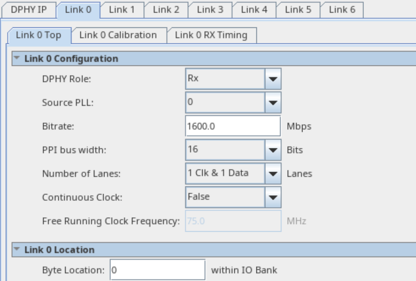
Figure 10. Link Top Tab
| Parameter Name | Description | Setting |
|---|---|---|
| D-PHY Role | Configure D-PHY mode as Tx or Rx. If not using the channel, please remain it as unused. | TX/RX/Unused. (Default value is Unused.) |
| Source PLL | Specify which PLL source to drive the link's clock. 0 = PLL from Bottom Sub bank 1 = PLL from Top Sub bank |
0 or 1. (Default value is 0.) |
| Bit Rate | Configure the MIPI D-PHY data rate. | D-Series: 150Mbps - 3500Mbps E-Series device group A: 150Mbps - 3500Mbps E-Series device group B: 150Mbps - 2500Mbps |
| PPI bus width | Set PPI bus width for data lanes in the link : 16 bits. | 16. |
| Number of Lanes | Set number of data lanes for the link : 1, 2, 4 or 8. | 1 Data & 1 Clk 2 Data & 1 Clk 4 Data & 1 Clk 8 Data & 1 Clk (Default is 1 Data & 1 Clk.) |
| Continuous Clock | Specify that the clock lane is continuous. | True or False. (Default value is False.) |
| Free Running Clock Frequency | Rx free running clock frequency in MHz. When calibration is enabled, this will be fixed to RX clock. | |
| Byte Location | Specifies D-PHY links BYTE location within the I/O bank. | 0-7. |
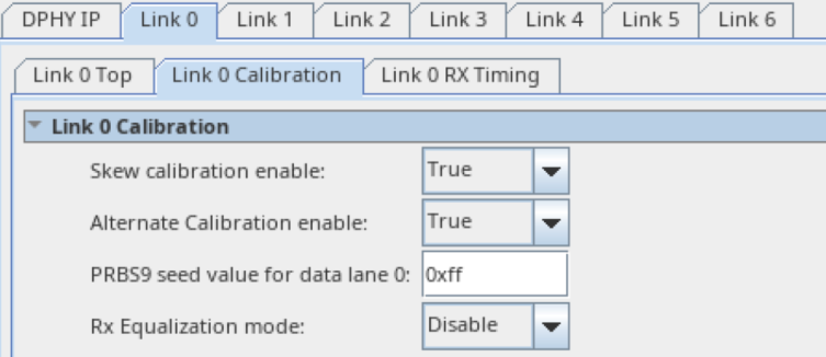
Link Calibration Configuration
On the Link Calibration tab you can enable the skew and alternate calibration functions and RX equilization mode. You can run simulation to validate which RX equalization mode suits your design intent.
Figure 11. Link Calibration Tab
| Parameter Name | Description | Setting |
|---|---|---|
| Skew Calibration Enable | Generate logic to support skew calibration. | True or False. (Default value is False.) |
| Alternate Calibration Enable | Generate logic to support alternate calibration. (Available when skew calibration mode is enabled.) | True or False. (Default value is False.) |
| PRBS9 seed value for data lane n | PRBS value for data lane used by Tx / Rx alt cal and test mode. (Available when Alternate Calibration is enabled.) | 0xFF |
| Rx Equalization mode | Rx Equalization mode | Disable or EQ SML or EQ MED or EQ LRG. Default value is Disable. |
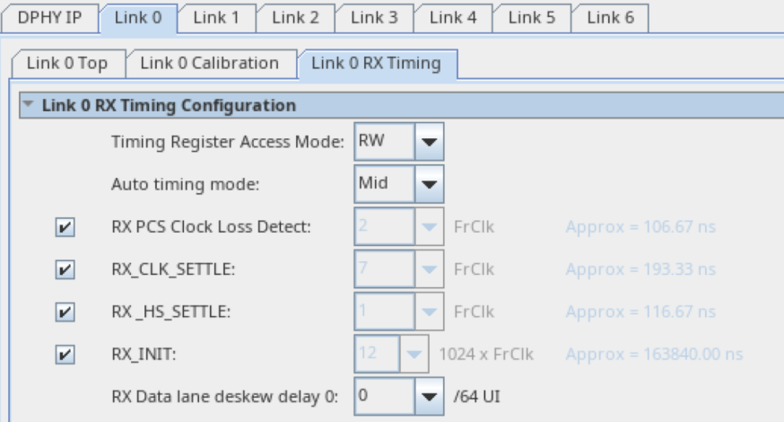
Link RX Timing Configuration
On the Link RX Timing tab you can configure the receive timing parameters.
Figure 12. Link RX Timing Tab
| Parameter Name | Description | Setting |
|---|---|---|
| Timing Register Access Mode | Set to implement timing registers as R/W or RO. When using R/W mode, more register consumes in logic element resources. |
RW or RO. (Default is RW.) |
| Auto Timing mode | Set Rx to be fixed at MID. Choose to use min timing, max timing or mid for default values of timing registers set to "Auto". All timing registers have a min specified timing, but not all have a max specified timing. For those with no max specified timing, max is set to register max value.
|
Max, Mid, or Min. (Default is Mid.) |
| RX PCS Clock Loss Detect | Timeout for D-PHY PCS to detect absence of Clock transitions and deassert RxClkActiveHS on the PPI bus. Min value should be equal to 3 x RX_CLK-period (in ns). This is different from the D-PHY specification TCLK-MISS. This will be used to clock gate MIPI RX forwarded clock delay computations (approx): - TRX_CLK_LOSS_DETECT = (RX_CLK_LOSS_DETECT + 6) * Core_CLK_period. |
0-255. (Default is 2.) |
| RX_CLK_SETTLE | Time interval during which the HS receiver should ignore any Clock Lane HS transitions, starting from the beginning of TCLK-PREPARE. Delay computation (approx): TRX-CLK-SETTLE = (RX_CLK_SETTLE + 6) * Core_CLK_period + 2 * RX_CLK_period. | 0-255. (Default is 7.) |
| RX_HS_SETTLE | Time interval during which the HS receiver shall ignore any Data Lane HS transitions, starting from the beginning of THS-PREPARE. The HS receiver shall ignore any Data Lane transitions before the minimum value, and the HS receiver shall respond to any Data Lane transitions after the minimum val Delay computation (approx): THS-SETTLE = (RX_HS_SETTLE + 7) * Core_CLK_period + RX_CLK_period. | 0-255. (Default is 1.) |
| RX_INIT | After power-up, the RX side PHY shall be initialized when the TX PHY drives a Stop State (LP-11) for a period longer than TINIT. RX side shall ignore all Line states prior to this Initialization period. | 0-255. (Default is 12.) |
| RX Data Lane deskew Delay 0 | Manual data Lane 0 deskew delay setting . | 0-63. (Default is 0.) |