Visible to Intel only — GUID: ldr1683035972064
Ixiasoft
6.2.1.1. IP_ID
6.2.1.2. IP_CAP
6.2.1.3. D0_CAP
6.2.1.4. DN_CAP
6.2.1.5. RX_CAP
6.2.1.6. TX_CAP
6.2.1.7. TX_PREAMBLE_LEN
6.2.1.8. D-PHY_CSR
6.2.1.9. TX_CLK_LANE_PS
6.2.1.10. RX_DLANE_ERR
6.2.1.11. SKEW_CAL_LEN_B0
6.2.1.12. SKEW_CAL_LEN_B1
6.2.1.13. SKEW_CAL_LEN_B2
6.2.1.14. SKEW_CAL_LEN_B3
6.2.1.15. ALT_CAL_LEN_B0
6.2.1.16. ALT_CAL_LEN_B1
6.2.1.17. ALT_CAL_LEN_B2
6.2.1.18. ALT_CAL_LEN_B3
6.2.1.19. CLK_CSR
6.2.1.20. CLK_STATUS
6.2.1.21. DLANE_CSR_0
6.2.1.22. DLANE_STATUS_0
6.2.1.23. RX_DLANE_DESKEW_DELAY_0
6.2.1.24. RX_DLANE_ERR_0
6.2.1.25. DLANE_CSR_1
6.2.1.26. DLANE_STATUS_1
6.2.1.27. RX_DLANE_DESKEW_DELAY_1
6.2.1.28. RX_DLANE_ERR_1
6.2.1.29. DLANE_CSR_2
6.2.1.30. DLANE_STATUS_2
6.2.1.31. RX_DLANE_DESKEW_DELAY_2
6.2.1.32. RX_DLANE_ERR_2
6.2.1.33. DLANE_CSR_3
6.2.1.34. DLANE_STATUS_3
6.2.1.35. RX_DLANE_DESKEW_DELAY_3
6.2.1.36. RX_DLANE_ERR_3
6.2.1.37. DLANE_CSR_4
6.2.1.38. DLANE_STATUS_4
6.2.1.39. RX_DLANE_DESKEW_DELAY_4
6.2.1.40. RX_DLANE_ERR_4
6.2.1.41. DLANE_CSR_5
6.2.1.42. DLANE_STATUS_5
6.2.1.43. RX_DLANE_DESKEW_DELAY_5
6.2.1.44. RX_DLANE_ERR_5
6.2.1.45. DLANE_CSR_6
6.2.1.46. DLANE_STATUS_6
6.2.1.47. RX_DLANE_DESKEW_DELAY_6
6.2.1.48. RX_DLANE_ERR_6
6.2.1.49. DLANE_CSR_7
6.2.1.50. DLANE_STATUS_7
6.2.1.51. RX_DLANE_DESKEW_DELAY_7
6.2.1.52. RX_DLANE_ERR_7
6.2.1.53. TX_LPX
6.2.1.54. TX_HS_EXIT
6.2.1.55. TX_LP_EXIT
6.2.1.56. TX_CLK_PREPARE
6.2.1.57. TX_CLK_ZERO
6.2.1.58. TX_CLK_POST
6.2.1.59. TX_CLK_PRE
6.2.1.60. TX_HS_PREPARE
6.2.1.61. TX_HS_ZERO
6.2.1.62. TX_HS_TRAIL
6.2.1.63. TX_INIT
6.2.1.64. TX_WAKE
6.2.1.65. RX_CLK_LOSS_DETECT
6.2.1.66. RX_CLK_SETTLE
6.2.1.67. RX_HS_SETTLE
6.2.1.68. RX_INIT
6.2.1.69. RX_CLK_POST
6.2.1.70. RX_CAL_REG_CTRL
6.2.1.71. RX_CAL_STATUS_D-PHY
6.2.1.72. RX_CAL_SKEW_W_START_MUX
6.2.1.73. RX_CAL_SKEW_W_END_MUX
6.2.1.74. RX_CAL_ALT_W_START_MUX
6.2.1.75. RX__CAL_ALT_W_END_MUX
6.2.1.76. RX_DESKEW_DELAY_MUX
6.2.1.77. RX_CAL_STATUS_LANE_MUX
6.2.1.78. PRBS_INIT_0
6.2.1.79. PRBS_INIT_1
6.2.1.80. PRBS_INIT_2
6.2.1.81. PRBS_INIT_3
6.2.1.82. PRBS_INIT_4
6.2.1.83. PRBS_INIT_5
6.2.1.84. PRBS_INIT_6
6.2.1.85. TX_TM_CONTROL
6.2.1.86. TX_MNL_IO_0
6.2.1.87. TX_MNL_D_LP_EN
6.2.1.88. RX_TM_CONTROL
6.2.2.1. TG_TOP_CTRL_0
6.2.2.2. TG_TOP_CTRL_1
6.2.2.3. TG_TOP_DONE
6.2.2.4. TG_TOP_FAIL
6.2.2.5. TG_TOP_TEST_EN
6.2.2.6. TG_TOP_TEST_LINK
6.2.2.7. TARGET_TEST_CNT
6.2.2.8. TCHK_CONTROL
6.2.2.9. TCHK_LINK_STATUS
6.2.2.10. HS_DONE_LANES
6.2.2.11. TCHK_LINK_ERR_STATUS
6.2.2.12. LANE_ERROR_SOT_LANES
6.2.2.13. CAL_ERROR_LANES
6.2.2.14. HS_ERR_LANES
6.2.2.15. HS_TEST_CNT
6.2.2.16. LPDT_TEST_CNT
6.2.2.17. TRIGGER_TEST_CNT
6.2.2.18. ULPS_TEST_CNT
6.2.2.19. TG_RX_OVRD_DATA_PAT
6.2.2.20. TG_RX_BIT_ERROR_CNT
6.2.2.21. TG_RX_HS_TXFER_CNT
6.2.2.22. TG_LINK_CONTROL
6.2.2.23. TG_INIT_CNT
6.2.2.24. TG_HS_LEN
6.2.2.25. TG_LP_LEN
6.2.2.26. TG_SKEW_CAL
6.2.2.27. TG_ALT_CAL
6.2.2.28. TG_PER_SKEW_CAL_LEN
6.2.2.29. TG_TEST_CNT
6.2.2.30. TG_OVRD_DATA_PAT
6.2.2.31. TG_TX_HS_TXFER_CNT
Visible to Intel only — GUID: ldr1683035972064
Ixiasoft
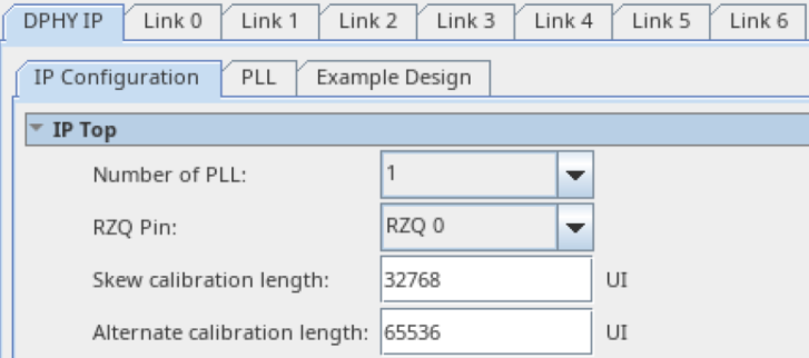
5.2. Configuring the D-PHY IP Tab
This topic describes the configuration of the general settings on the D-PHY IP tab in the parameter editor.
Figure 8. D-PHY IP Configuration Tab
| Parameter Name | Description | Setting |
|---|---|---|
| Number of PLL | Set number of PLL to use for clock generation. The IP can use up to 2 PLLs to share among the different D-PHY links. The bit rates of the D-PHY links has to be the same to share a PLL. | 1 or 2. (Default value is 1.) |
| RZQ Pin | Set RZQ pin location to use for the D-PHY IP. | RZQ0 or RZQ1. (Default value is RZQ0.) Pin 38 in one I/O bank is RZQ0 and pin 62 is RZQ1. Pin 38 reserves BYTE LOCATION 3, and pin 62 reserves BYTE LOCATION 5. |
| Skew calibration length | Length of initial skew calibration pattern automatically generated by D-PHY TX IP when SKEW_CAL_EN = 1. This is done automatically after the t INIT period. When SKEW_CAL_EN = 0, protocol IP is responsible to drive TxSkewCalHS to generate init skew sequence. SKEW_CAL_LEN is ignored by D-PHY RX IP. | 32768 (This is the default value and the minimum.) |
| Alternate calibration length | Length of alternate calibration pattern automatically generated by D-PHY TX IP when ALT_CAL_EN = 1. This is done automatically after the init skew. When SKEW_CAL_EN = 0, protocol IP is responsible to drive TxAlTCalHS to generate alt cal sequence.ALT_CAL_LEN is ignored by D-PHY RX IP. | 65536 (This is the default value and the minimum.) |
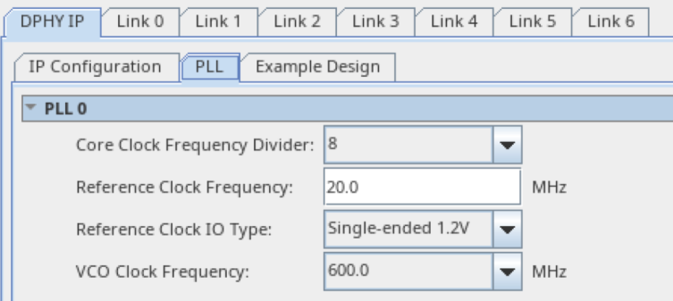
D-PHY IP PLL Tab
On the PLL tab, you configure the PLL settings such as core clock divider, PLL reference clock frequency, I/O standard selection, and VCO clock frequency.
Figure 9. D-PHY IP PLL Tab
| Parameter Name | Description | Setting |
|---|---|---|
| Core clock frequency divider | Set core clock frequency divider to generate core clock from VCO output. MIPI only supports divided by 4 or 8. | 4 or 8. (Default value is 8.) |
| Reference clock frequency | PLL reference clock frequency. | 10MHz - 300MHz. (Default value is 20MHz.) |
| Reference clock I/O type | Reference Clock I/O standard. | Single Ended 1.2V, LVDS 1.2V Single Ended 1.1V, LVDS 1.1V . |
| Share Reference Clock I/O | Enable PLL1 share reference clock with PLL0. | True or False. (Default value is True.) |
| VCO Clock Frequency | Sets the VCO clock frequency for PLL. - MIPI TX with bitrate > 1.2Gbps: VCO freq = 1/2 bit rate. - MIPI TX with bitrate 1.2Gbps: VCO freq = 1/2 bitrate * Tx bitrate divider (1, 2, 4 of 8). - MIPI RX with skew calibration disabled: no dependency between VCO freq and bit rate. -MIPI RX with skew calibration enabled: VCO freq = 1/2 bitrate |
600MHz - 1740MHz. |