AXI Streaming Intel® FPGA IP for PCI Express* User Guide
Visible to Intel only — GUID: wjl1698183040535
Ixiasoft
Visible to Intel only — GUID: wjl1698183040535
Ixiasoft
3.6.1. Simulating the Design Example
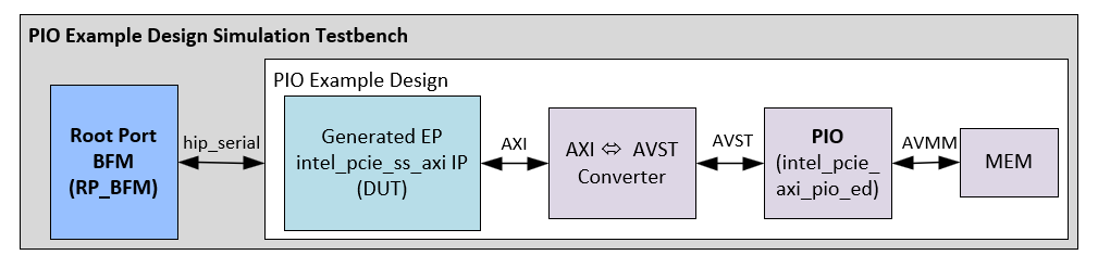
The simulation setup involves the use of a Root Port Bus Functional Model (BFM) to exercise the AXI Streaming Intel® FPGA IP for PCI Express* (DUT) as shown in the following figure.
The following flow diagram shows the steps to simulate the design example:
- Change to the testbench simulation directory, <project_directory>/pcie_ss_ed_tb/pcie_ss_ed_tb/sim/<EDA_vendor>/simulator.
- Run the simulation script for the simulator of your choice. Refer to the table below.
- Analyze the results.
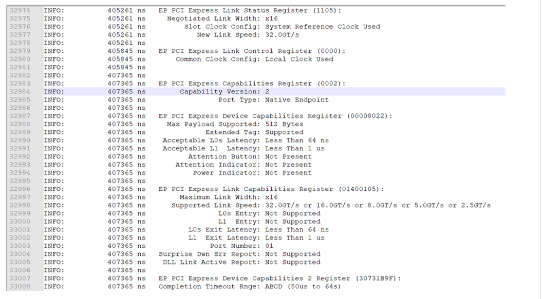
The following figure shows the link status information for a Gen5 x16 Endpoint simulation:
After a successful simulation, the simulation.log file contains a "successful completion" message.
This testbench simulates up to a Gen5 x16 variant.