AXI Streaming Intel® FPGA IP for PCI Express* User Guide
Visible to Intel only — GUID: asr1719530768112
Ixiasoft
Visible to Intel only — GUID: asr1719530768112
Ixiasoft
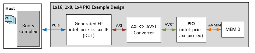
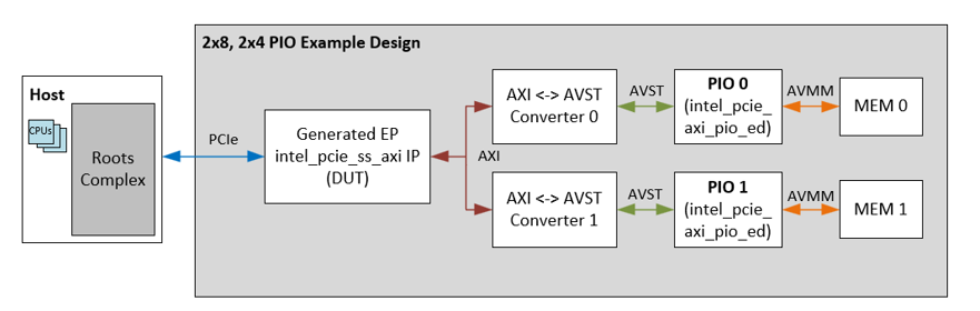
3.4.1. Functional Description for the Programmed Input/Output (PIO) Design Example
The Programmed Input/Output (PIO) design example performs memory transfers from a host processor to a target device. In this design example, the host processor performs Memory Read (MemRd) and Memory Write (MemWr) Transaction Layer Packets (TLPs). Note that this design example does not support back-to-back transactions from the host processor since the design is intended to showcase single-dword transactions.
The PIO design example automatically creates the files necessary to simulate and compile in the Quartus® Prime software. The design example covers a wide range of parameters. However, it does not cover all possible parameterizations of the AXI Streaming IP for PCI Express.
This design example supports the following configurations:
| Port Mode | Link Width | Link Speed | HIP Data Width (Bits) | Application Data Width (Bits) | Compact/HIP Native Mode | Design Example Support |
|---|---|---|---|---|---|---|
| Endpoint | 1x16 | Gen5 | 1024 (4 x 256) | 1024 (4 x 256) | HIP Native | SCTH |
| 2x8 | Gen5 | 512 (2 x 256) | 512 (2 x 256) | HIP Native | SCTH | |
| Root Port | N/A | N/A | N/A | N/A | N/A | N/A |
| TL Bypass | N/A | N/A | N/A | N/A | N/A | N/A |