7.2. Hardware
This section describes the Example Design in detail.
A top-level view of the design example is shown in FPGA AI Suite Example Design Top Level.
The instances of FPGA AI Suite IP are on the right (dla_top.sv). All communication between the FPGA AI Suite IP systems and the outside occurs via the FPGA AI Suite IP DMA. The FPGA AI Suite IP DMA provides a CSR (which also has interrupt functionality) and reader/writer modules which read/write from DDR.
The host communicates with the board through the PCIe* protocol. The host can do the following things:
- Read and write the on-board DDR memory (these reads/writes do not go through FPGA AI Suite IP).
- Read/write to the FPGA AI Suite IP DMA CSR of the instances.
- Receive interrupt signals from the FPGA AI Suite IP DMA CSR of both instances.
Each FPGA AI Suite IP instance can do the following things:
- Read/write to its DDR bank.
- Send interrupts to the host through the interrupt interface.
- Receive reads/writes to its DMA CSR.
From the perspective of the FPGA AI Suite, external connections are to the PCIe* interface and to the on-board DDR4 memory. The DDR memory is connected directly to mem.qsys block, while the PCIe interface is converted into Avalon® memory mapped (MM) interfaces in pcie_ed.qsys block for communication with the mem.qsys block.
The mem.qsys blocks arbitrate the connections to DDR memory between the reader/writer modules in FPGA AI Suite IP and reads/writes from the host. Each FPGA AI Suite IP instance in this design has access to only one of the DDR banks. This design decision implies that the number simultaneous FPGA AI Suite IP instances that can exist in the design is limited to the number of DDR blocks available on the board. Adding an additional arbiter would relax this restriction and allow additional FPGA AI Suite IP instances.
Much of board.qsys operates using the Avalon® Memory-mapped (MM) interface protocol. The FPGA AI Suite DMA uses AXI protocol, and board.qsys has Avalon® MM interface to AXI adapters just before each interface is exported to the FPGA AI Suite IP (so that outside of the Platform Designer system it can be connected to FPGA AI Suite IP). Clock crossing is also handled inside of board.qsys. For example, the host interface must be brought to the DDR clock to talk with the FPGA AI Suite IP CSR.
There are three clock domains: host clock, DDR clock, and the FPGA AI Suite IP clock. The PCIe* logic runs on the host clock. FPGA AI Suite DMA and the platform adapters run on the DDR clock. The rest of FPGA AI Suite IP runs on the FPGA AI Suite IP clock.
FPGA AI Suite IP protocols:
- Readers and Writers: 512-bit data (width configurable), 32-bit address AXI4 interface, 16-word max burst (width fixed).
- CSR: 32-bit data, 11-bit address
Figure 3. FPGA AI Suite Example Design Top Level
The board.qsys block contains two major elements; the pcie_ed.qsys block and the mem.qsys blocks. The pcie_ed.qsys block interfaces between the host PCIe data and the mem.qsys blocks. The mem.qsys blocks interface between DDR memory, the readers/writers, and the host read/write channels.
- Host read is used to read data from DDR memory and send it to the host.
- Host write is used to read data from the host into DDR memory.
- The MMIO interface performs several functions:
- DDR read and write transactions are initiated by the host via the MMIO interface
- Reading from the AFU ID block. The AFU ID block identifies the AFU with a unique identifier and is required for the OPAE driver.
- Reading/writing to the DLA DMA CSRs where each instance has its own CSR base address.
Note: Avalon® MM/AXI4 adapters in Platform Designer might not close timing.
Platform Designer optimizes for area instead of fMAX by default, so you might need to change the interconnect settings for the inferred Avalon® MM/AXI4 adapter. For example, we made some changes as shown in the following figure.
Figure 4. Adjusting the Interconnect Settings for the Inferred Avalon® MM/AXI4 Adapter to Optimize for fMAX Instead of Area.
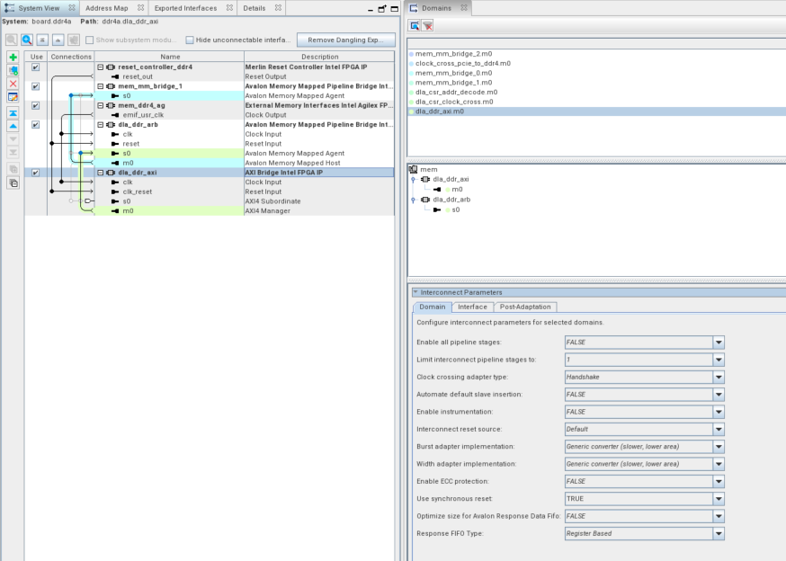
Note: This enables timing closure on the DDR clock.
To access the view in the above figure:
- Within the Platform Designer GUI choose View -> Domains. This brings up the Domains tab in the top-right window.
- From there, choose an interface (for example, dla_ddr_axi).
- For the selected interface, you can adjust the interconnect parameters, as shown on the bottom-right pane.
- In particular, we needed to change Burst adapter implementation from Generic converter (slower, lower area) to Per-burst-type converter (faster, higher area) to close timing on the DDR clock.
This was the only change needed to close timing, however it took several rounds of experimentation to determine this was the setting of importance. Depending on your system, other settings might need to be tweaked.