Intel® Quartus® Prime Pro Edition User Guide: Getting Started
ID
683463
Date
12/12/2022
Public
A newer version of this document is available. Customers should click here to go to the newest version.
3.1. Creating a New FPGA Design Project
3.2. Viewing Basic Project Information
3.3. Intel® Quartus® Prime Project Contents
3.4. Managing Project Settings
3.5. Managing Logic Design Files
3.6. Managing Timing Constraints
3.7. Integrating Other EDA Tools
3.8. Exporting Compilation Results
3.9. Migrating Projects Across Operating Systems
3.10. Archiving Projects
3.11. Command-Line Interface
3.12. Managing Projects Revision History
3.8.1. Exporting a Version-Compatible Compilation Database
3.8.2. Importing a Version-Compatible Compilation Database
3.8.3. Creating a Design Partition
3.8.4. Exporting a Design Partition
3.8.5. Reusing a Design Partition
3.8.6. Viewing Quartus Database File Information
3.8.7. Clearing Compilation Results
4.1. Design Planning
4.2. Create a Design Specification and Test Plan
4.3. Plan for the Target Device or Board
4.4. Plan for Intellectual Property Cores
4.5. Plan for Standard Interfaces
4.6. Plan for Device Programming
4.7. Plan for Device Power Consumption
4.8. Plan for Interface I/O Pins
4.9. Plan for other EDA Tools
4.10. Plan for On-Chip Debugging Tools
4.11. Plan HDL Coding Styles
4.12. Plan for Hierarchical and Team-Based Designs
4.13. Design Planning Revision History
5.1. IP Catalog and Parameter Editor
5.2. Installing and Licensing Intel® FPGA IP Cores
5.3. IP General Settings
5.4. Adding IP to IP Catalog
5.5. Best Practices for Intel® FPGA IP
5.6. Specifying the IP Core Parameters and Options ( Intel® Quartus® Prime Pro Edition)
5.7. IP Core Generation Output ( Intel® Quartus® Prime Pro Edition)
5.8. Scripting IP Core Generation
5.9. Modifying an IP Variation
5.10. Upgrading IP Cores
5.11. Simulating Intel® FPGA IP Cores
5.12. Generating Simulation Files for Platform Designer Systems and IP Variants
5.13. Synthesizing IP Cores in Other EDA Tools
5.14. Instantiating IP Cores in HDL
5.15. Support for the IEEE 1735 Encryption Standard
5.16. Introduction to Intel FPGA IP Cores Revision History
6.2.1. Modify Entity Name Assignments
6.2.2. Resolve Timing Constraint Entity Names
6.2.3. Verify Generated Node Name Assignments
6.2.4. Replace Logic Lock (Standard) Regions
6.2.5. Modify Signal Tap Logic Analyzer Files
6.2.6. Remove References to .qip Files
6.2.7. Remove Unsupported Feature Assignments
6.4.1. Verify Verilog Compilation Unit
6.4.2. Update Entity Auto-Discovery
6.4.3. Ensure Distinct VHDL Namespace for Each Library
6.4.4. Remove Unsupported Parameter Passing
6.4.5. Remove Unsized Constant from WYSIWYG Instantiation
6.4.6. Remove Non-Standard Pragmas
6.4.7. Declare Objects Before Initial Values
6.4.8. Confine SystemVerilog Features to SystemVerilog Files
6.4.9. Avoid Assignment Mixing in Always Blocks
6.4.10. Avoid Unconnected, Non-Existent Ports
6.4.11. Avoid Illegal Parameter Ranges
6.4.12. Update Verilog HDL and VHDL Type Mapping
3.2.3.1. Viewing Synthesis Warning Messages
Warning messages may contain hierarchies. In Compilation Report > Synthesis > Messages window, you can view hierarchical warning messages up to any level including the parent and child messages. For each message, you can view its source, file location, line number, and message ID by selecting appropriate column under Message Column (right-click on a message in the Message panel as shown in the following image and click Message Column).
Figure 18. Synthesis Warning Messages (Two levels)
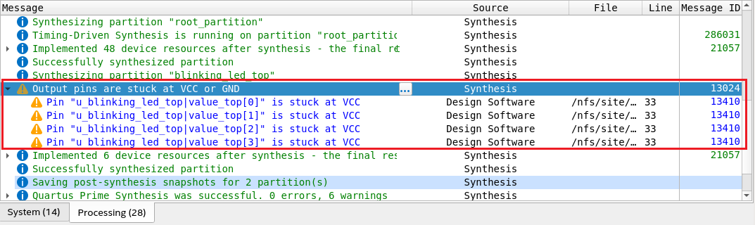
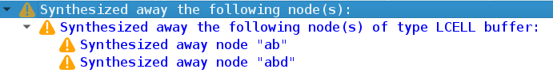
Figure 19. Example of Synthesis Warning Messages With Three Levels
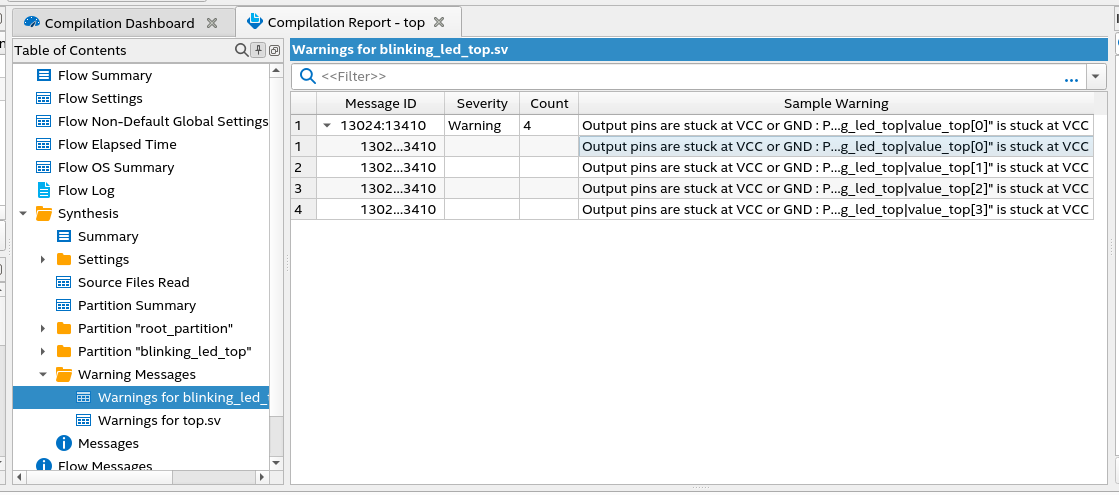
In Compilation Report > Synthesis > Warning Messages, you can view a comprehensive list of synthesis warning messages for each source file included in your design. You can view all child warning messages hidden within a parent warning message by expanding the collapsible rows. To view the location of each warning, perform these steps:
- Right-click on the message.
- Select the Locate Node option.
- Select the desired tool to view the node.
Note: In the source file-specific warning messages window, messages are hierarchical in nature and display up to three levels. If the warning messages go deeper than three levels, use the Message (View > Messages) window to view them.
In the source file-specific warning messages window, hierarchical messages are displayed with message IDs and sample warning messages that are a combination of the parent and child messages.
Figure 20. Synthesis Warning Messages for Each Source File