Intel® Stratix® 10 Avalon® Streaming (Avalon-ST) IP for PCIe* Design Example User Guide
2.1. Functional Description for PIO Design Example
The testbench illustrates PIO traffic between the host and Endpoint. The PIO design example consists of memory transfers from a host processor to a target device. In this example, the host processor issues single-dword MemRd and MemWr TLPs.
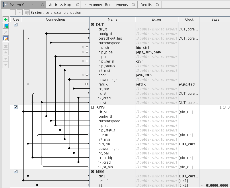
The Endpoint (DUT) and PIO application (APPS) perform the necessary translation between the PCI Express TLPs and simple Avalon-MM reads and writes to memory.
The PIO testbench includes the following components:
- The Root Port BFM that drives downstream TLPs to the Endpoint.
Note: This Intel Root Port BFM provides a simple method to do basic testing of the Application Layer logic that interfaces to the DUT. However, the testbench and Root Port BFM are not intended to be a substitute for a full verification environment. To thoroughly test your application, obtain commercially available PCI Express verification IP and tools, or do your own extensive hardware testing or both.
- The Generated PCIe Endpoint Variant (DUT) with the parameters you specified. This component drives TLP data received to the PIO application. For more details on this component, refer to the Intel Stratix 10 Avalon Streaming (Avalon-ST) and Single Root I/O Virtualization (SR-IOV) Interface for PCI Express Solutions User Guide.
- The PIO Application (APPS) component. Along with some additional logic, it translates Avalon-ST data to Avalon-MM data for writes and reads to the on-chip memory.
- For variants up to Gen3 x8, an on-chip memory (MEM) stores data. Gen3 x16 variants include the memory in the APPs component.
The test program writes and reads back data to 0x00000040 in the on-chip memory. It compares data read to the expected result. The test reports, "Simulation stopped due to successful completion" if no errors occur.
Figure 6. Platform Designer System Contents for Stratix® 10 PCI Express PIO Design Example The Platform Designer generates this design for up to Gen3 x16 variants.

