3. IP Parameter Settings

| Parameter | Supported Values | Default Setting | Description |
|---|---|---|---|
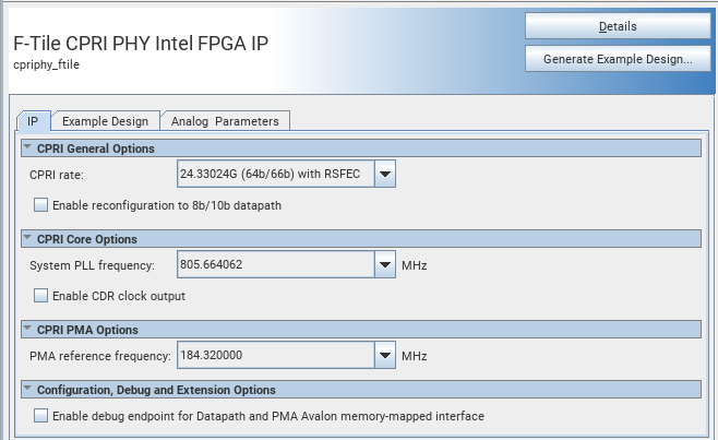
| CPRI General Options | |||
| CPRI Rate |
|
24.33024G (64b/66b) with RS-FEC | Selects the CPRI data rate. The hard RS-FEC block is included in the core if you select 10.1376, 12.1651, and 24.33024 Gbps (64b/66b) with the RS-FEC option. |
| Enable Reconfiguration to 8b/10b Datapath |
|
Off | Turn on this parameter if you plan to reconfigure the CPRI line rate of your channels from 64b/66b datapath rates to 8b/10b datapath rates at run-time. If this option is not enabled, the CPRI IP core uses fewer resources, and you cannot change to 8b/10b datapath rates at run-time. |
| CPRI Core Options | |||
| System PLL Frequency |
|
805.664062 MHz | Select the System PLL frequency for your IP. |
| Enable CDR Clock Output |
|
Off | Turn on this parameter to enable CDR reference clock output. o_cdr_divclk = refclk/N Refer to the Required Clock Frequencies for exact values. |
| CPRI PMA Options | |||
| PMA Reference Frequency |
|
184.32 MHz | Reference clock frequency support:
|
| Configuration, Debug, and Extension Option | |||
| Enable Debug Endpoint for Datapath and PMA Avalon Memory-Mapped Interface |
|
Off | When turned On, the F-Tile CPRI PHY Intel FPGA IP core includes an embedded Debug Endpoint that internally connects the Avalon memory-mapped agent interface. The Debug Endpoint can access the reconfiguration space of the Datapath and PMA interface block. it can perform certain tests and debug functions through JTAG using the System Console. This option may require that you include a jtag_debug link in the system. |
For parameters in the Example Design tab, refer to the device specific F-Tile CPRI PHY Intel FPGA IP Design Example User Guide.
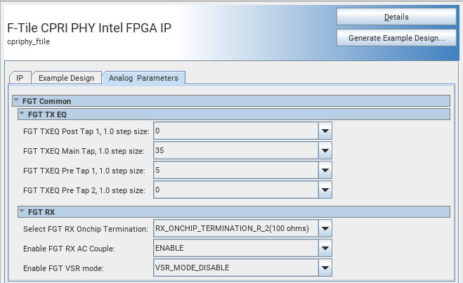
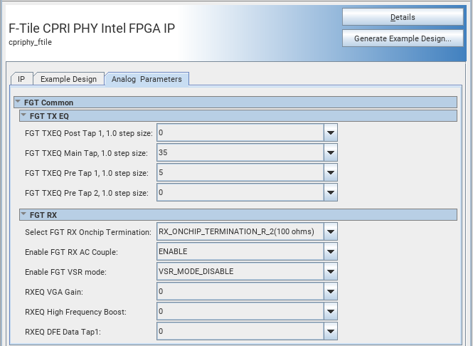
For parameters in the Analog Parameters tab, refer to the F-tile Architecture and PMA and FEC Direct PHY IP User Guide.
- RXEQ VGA Gain
- RXEQ High Frequency Boost
- RXEQ DFE Data Tap1


The default and recommended analog parameters values are shown in the table below:
| Parameter | Value |
|---|---|
| FGT TXEQ Post Tap 1, 1.0 step size | 0 |
| FGT TXEQ Main Tap 1.0 step size | 35 |
| FGT TXEQ Pre Tap 1, 1.0 step size | 5 |
| FGT TXEQ Pre Tap 2, 1.0 step size | 0 |
| FGT RX Onchip Termination | RX_ONCHIP_TERMINATION_R_2 (100 ohms) |
| Enable FGT RX AC Couple | ENABLE |
| Enable FGT VSR mode |
|
| RXEQ VGA Gain | 0 (Required only when CPRI rate is 6.1440Gbps and below) |
| RXEQ High Frequency Boost | 0 (Required only when CPRI rate is 6.1440Gbps and below) |
| RXEQ DFE Data Tap1 | 0 (Required only when CPRI rate is 6.1440Gbps and below) |
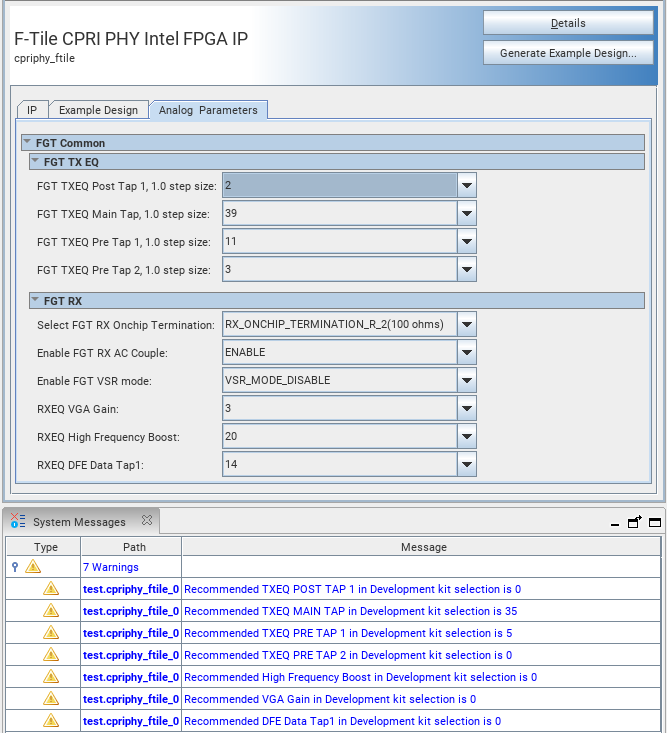
In the Example Design tab, if you select Target Development Kit to be Intel Agilex 7 FPGA I-Series Transceiver-SoC Development Kit, and you configure analog parameters other than the default and recommended values, you will see warnings to recommend you set to the default values.
