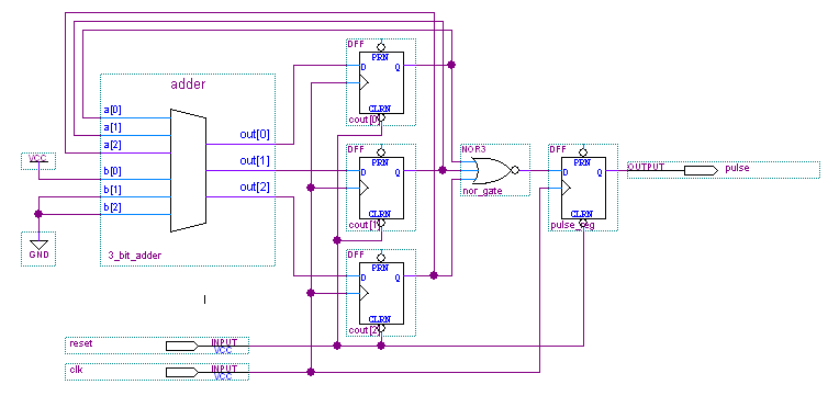
A pulse generator in a design should not generate pulses in one of the following ways:
- By increasing the width of a glitch using a 2-input AND, NAND, OR, or NOR gate, where the source for the two gate inputs are the same, but the design inverts the source for one of the gate inputs.
- Using a register where the register output drives the register's own asynchronous reset signal through an delay chain (one or more consecutive nodes that act as a buffer for creating intentional delay).
These pulse generators are asynchronous, where the generated pulse width is always equal to the clock period. As a result, the pulse widths depend on circuit delay. For example, the pulse width generated by a pulse generator that uses a 2-input AND gate depends on the relative delays of the path that drives the AND gate directly and the path that the design inverts before driving the AND gate.
The following image shows an example of a recommended pulse generator that is implemented in a synchronous manner:
