Intel Demonstrates Breakthroughs in Next-Generation Transistor Scaling for Future Nodes

video grab from IEDM 120923 #a1425908 /content/dam/www/central-libraries/us/en/videos/2023-12/newsroom-iedm-2023-original.mp4 /content/www/us/en/newsroom/news/research-advancements-extend-moore-law.html
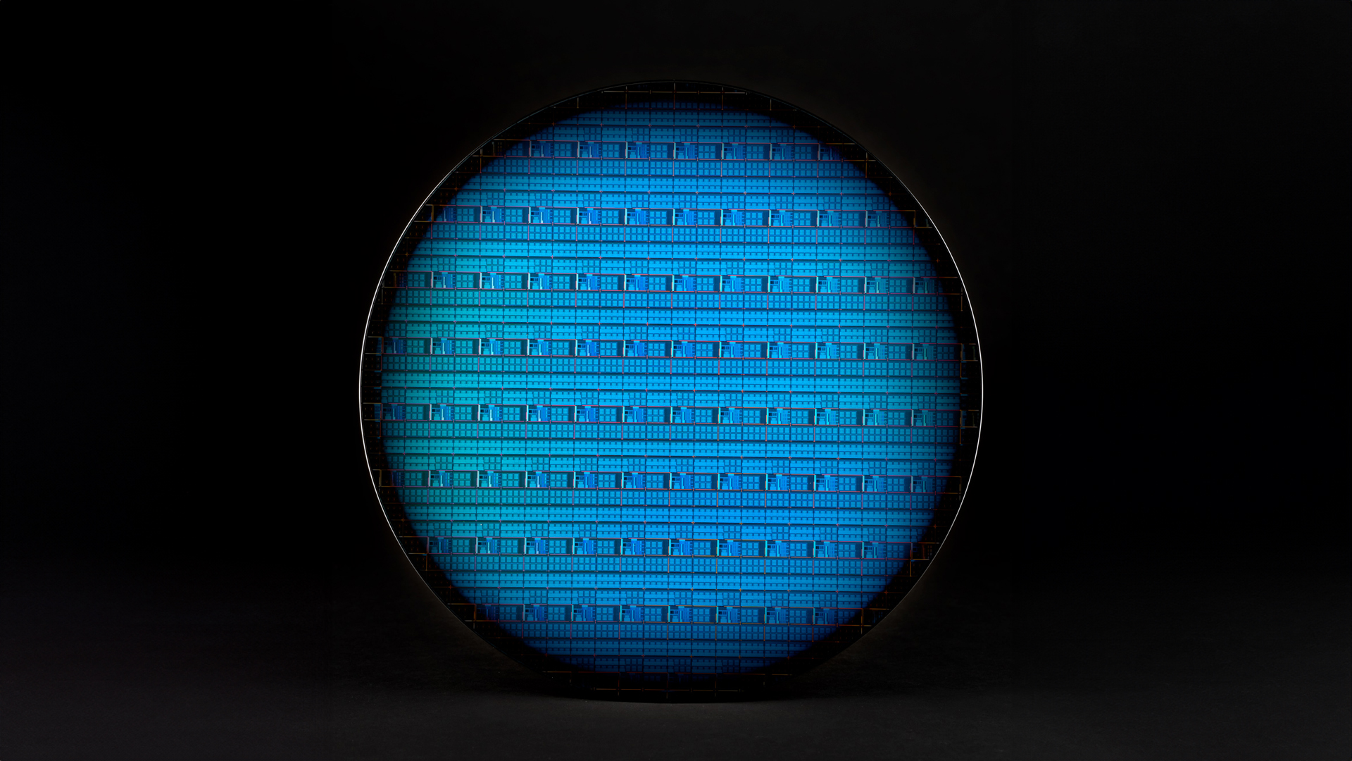
At IEDM 2023, Intel showcases 3D stacked CMOS transistors combined with backside power and direct backside contact – first-of-a-kind advancements that will extend Moore’s Law.
What’s New: Today, Intel unveiled technical breakthroughs that maintain a rich pipeline of innovations for the company’s future process roadmap, underscoring the continuation and evolution of Moore’s Law. At the 2023 IEEE International Electron Devices Meeting (IEDM), Intel researchers showcased advancements in 3D stacked CMOS (complementary metal oxide semiconductor) transistors combined with backside power and direct backside contacts. The company also reported on scaling paths for recent R&D breakthroughs for backside power delivery, such as backside contacts, and it was the first to demonstrate successful large-scale 3D monolithic integration of silicon transistors with gallium nitride (GaN) transistors on the same 300 millimeter (mm) wafer, rather than on package.
“As we enter the Angstrom Era and look beyond five nodes in four years, continued innovation is more critical than ever. At IEDM 2023, Intel showcases its progress with research advancements that fuel Moore’s Law, underscoring our ability to bring leading-edge technologies that enable further scaling and efficient power delivery for the next generation of mobile computing.”
Why It Matters: Transistor scaling and backside power are key to helping meet the exponentially increasing demand for more powerful computing. Year after year, Intel meets this computing demand, demonstrating that its innovations will continue to fuel the semiconductor industry and remain the cornerstone of Moore’s Law. Intel’s Components Research group consistently pushes the boundaries of engineering by stacking transistors, taking backside power to the next level to enable more transistor scaling and improved performance, as well as demonstrating that transistors made of different materials can be integrated on the same wafer.
Recent process technology roadmap announcements highlighting the company’s innovation in continued scaling – including PowerVia backside power, glass substrates for advanced packaging and Foveros Direct – originated in Components Research and are expected to be in production this decade.
How We Do It: At IEDM 2023, Components Research showed its commitment to innovating new ways of putting more transistors on silicon while achieving higher performance. Researchers have identified key R&D areas necessary to continue scaling by efficiently stacking transistors. Combined with backside power and backside contacts, these will be major steps forward in transistor architecture technology. Along with improving backside power delivery and employing novel 2D channel materials, Intel is working to extend Moore’s Law to a trillion transistors on a package by 2030.
Intel delivers industry-first, breakthrough 3D stacked CMOS transistors combined with backside power and backside contact:
- Intel’s latest transistor research presented at IEDM 2023 shows an industry first: the ability to vertically stack complementary field effect transistors (CFET) at a scaled gate pitch down to 60 nanometers (nm). This allows area efficiency and performance benefits by stacking transistors. It is also combined with backside power and direct backside contacts. It underscores Intel’s leadership in gate-all-around transistors and showcases the company’s ability to innovate beyond RibbonFET, putting it ahead of the competition.
Intel Ireland wins Prestigious NISO Safety Awards
3D Stacking of CMOS Transistor
Intel’s latest transistor research presented at IEDM 2023 shows an industry first: the ability to vertically stack complementary field effect transistors (CFET) at a scaled gate pitch down to 60 nanometers (nm). It underscores Intel’s leadership in gate-all-around transistors and showcases the company’s ability to innovate beyond RibbonFET, putting it ahead of the competition. (Credit: Intel Corporation)
Intel goes beyond five nodes in four years and identifies key R&D areas needed to continue transistor scaling with backside power delivery:
- Intel’s PowerVia will be manufacturing-ready in 2024, which will be the first implementation of backside power delivery. At IEDM 2023, Components Research identified paths to extend and scale backside power delivery beyond PowerVia, and the key process advances required to enable them. In addition, this work also highlighted the use of backside contacts and other novel vertical interconnects to enable area-efficient device stacking.
Intel is first to successfully integrate silicon transistors with GaN transistors on the same 300 mm wafer and demonstrate it performs well:
- At IEDM 2022, Intel focused on performance enhancements and building a viable path to 300 mm GaN-on-silicon wafers. This year, the company is making advancements in process integration of silicon and GaN. Intel has now successfully demonstrated a high-performance, large-scale integrated circuit solution – called “DrGaN” – for power delivery. Intel researchers are the first to show that this technology performs well and can potentially enable power delivery solutions to keep pace with the power density and efficiency demands of future computing.
Intel advances R&D in the 2D transistor space for future Moore’s Law scaling:
- Transition metal dichalcogenide (TMD) 2D channel materials offer a unique opportunity for scaled transistor physical gate length below 10nm. At IEDM 2023, Intel will demonstrate prototypes of high-mobility TMD transistors for both NMOS (n-channel metal oxide semiconductor) and PMOS (p-channel metal oxide semiconductor), the key components of CMOS. Intel will also present the world’s first gate-all-around (GAA) 2D TMD PMOS transistor, and the world’s first 2D PMOS transistor fabricated on a 300 mm wafer.
More Context: Introducing New RibbonFET and PowerVia Technologies (Video)
The Small Print:
All product and service plans and roadmaps are subject to change without notice. Any forecasts of goods and services needed for Intel's operations are provided for discussion purposes only. Intel will have no liability to make any purchase in connection with forecasts published in this document. Code names are often used by Intel to identify products, technologies, or services that are in development and usage may change over time. No license (express or implied, by estoppel or otherwise) to any intellectual property rights is granted by this document. Product and technology performance varies by use, configuration and other factors. Learn more at www.Intel.com/PerformanceIndex and www.Intel.com/ProcessInnovation.
Reference to research results, including comparisons to technologies, products, process or package performance are estimates and do not imply availability. Release dates and/or capabilities referenced may vary by use, configuration and other factors. The products and services described may contain defects or errors which may cause deviation from published specifications. Current characterized errata are available on request. Intel disclaims all express and implied warranties, including without limitation, the implied warranties of merchantability, fitness for a particular purpose, and non-infringement, as well as any warranty arising from course of performance, course of dealing, or usage in trade.
Statements in this document that refer to future plans or expectations are forward-looking statements. These statements are based on current expectations and involve many risks and uncertainties that could cause actual results to differ materially from those expressed or implied in such statements. For more information on the factors that could cause actual results to differ materially, see our most recent earnings release and SEC filings at www.intc.com.


