Visible to Intel only — GUID: ksw1487372637420
Ixiasoft
Visible to Intel only — GUID: ksw1487372637420
Ixiasoft
8.2. Write DMA Example
This example moves three data blocks from the Avalon-MM address space to the PCIe address space (system memory).

The following figures illustrate the location and size of the data blocks in the PCIe and Avalon-MM address spaces and the descriptor table format. In this example, the value of RD_TABLE_SIZE is 127.
The descriptor table includes 128 entries. The status table precedes a variable number of descriptors in memory. The Read and Write Status and Descriptor Tables are at the address specified in the Read Descriptor Base Register and Write Descriptor Base Register, respectively.
- Software allocates memory for Write Descriptor Status table and Write Descriptor Controller table in host memory. The memory allocation requires the following calculation:
- Each entry in the write status table is 4 bytes. The 128 write entries require 512 bytes of memory.
- Each descriptor is 32 bytes. The three descriptors require 96 bytes of memory.
Note: To avoid a possible overflow condition, allocate the memory needed for the number of descriptors supported by RD_TABLE_SIZE, rather than the initial number of descriptors.
The total memory that software must allocate for the status and descriptor tables is 608 bytes. The Write Descriptor Controller Status table follows the Read Descriptor Controller Status table. The Read Status table entries require 512 bytes of memory. Consequently, the Write Descriptor Status table begins at 0xF000_0200. - Program the Write Descriptor Controller table starting at offset 0x200 from the address shown in Data Blocks to Transfer from Avalon-MM Address Space to PCIe System Memory Using Write DMA . The three blocks of data require three descriptors.
- Program the Write Descriptor Controller register Write Status and Descriptor Base register with the starting address of the descriptor table.
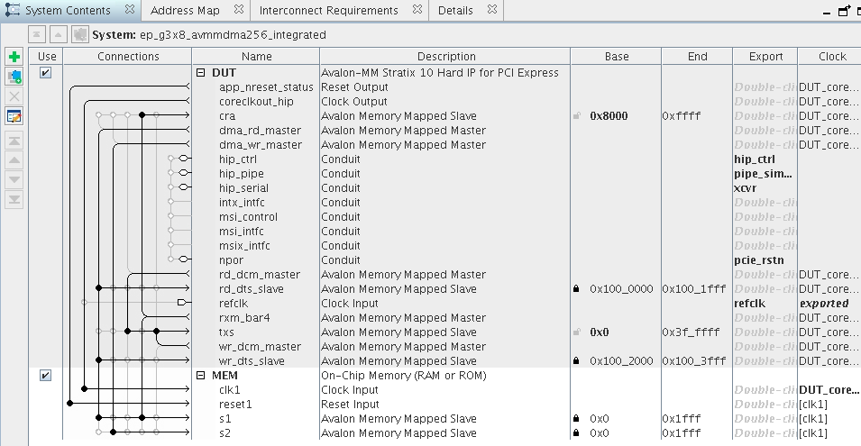
- Program the Write Descriptor Controller Write Descriptor FIFO Base with the starting address of the on-chip write descriptor table FIFO. This is the base address for the wr_dts_slave port in Platform Designer. In this example, the address is 0x0100_0200.
Figure 66. Address of the On-Chip Write FIFO
- To get status updates for each descriptor, program the Write Descriptor Controller register WR_CONTROL with 0x1. This step is optional.
- Program the Write Descriptor Controller register WR_DMA_LAST_PTR with the value 3. Writing this register triggers the Write Descriptor Controller descriptor table fetch process. Consequently, writing this register must be the last step in setting up DMA transfers.
- The host waits for the MSI interrupt. The Write Descriptor Controllers sends MSI to the host after completing the last descriptor. The Write Descriptor Controller also writes the Update.
- If there are additional blocks of data to move, complete the following steps to set up additional transfers.
- Program the descriptor table starting from memory address 0xF000_0200 + (<previous last descriptor pointer> * 0x20). In this case the descriptor pointer was 3.
- Program the Write Descriptor Controller register WR_DMA_LAST_PTR with previous_value (3 in this case) + number of new descriptors. Writing this register triggers the Write Descriptor Controller descriptor table fetch process. Consequently, writing this register must be the last step in setting up DMA transfers.
Note: When WR_DMA_LAST_PTR approaches the WR_TABLE_SIZE, be sure to program the WR_DMA_LAST_PTR with a value equal to WR_TABLE_SIZE. Doing so, ensures that the rollover to the first descriptor at the lowest offset occurs, (0xF000_0200 in this example). Refer to the description of theWR_DMA_LAST_PTR in the Write DMA Descriptor Controller Registers section for further information about programming the WR_DMA_LAST_PTR register.