Visible to Intel only — GUID: nkc1488904847754
Ixiasoft
Answers to Top FAQs
1. Hyperflex® FPGA Architecture Introduction
2. Hyperflex® Architecture RTL Design Guidelines
3. Compiling Hyperflex® Architecture Designs
4. Design Example Walk-Through
5. Retiming Restrictions and Workarounds
6. Optimization Example
7. Hyperflex® Architecture Porting Guidelines
8. Appendices
9. Hyperflex® Architecture High-Performance Design Handbook Archive
10. Hyperflex® Architecture High-Performance Design Handbook Revision History
2.4.2.1. High-Speed Clock Domains
2.4.2.2. Restructuring Loops
2.4.2.3. Control Signal Backpressure
2.4.2.4. Flow Control with FIFO Status Signals
2.4.2.5. Flow Control with Skid Buffers
2.4.2.6. Read-Modify-Write Memory
2.4.2.7. Counters and Accumulators
2.4.2.8. State Machines
2.4.2.9. Memory
2.4.2.10. DSP Blocks
2.4.2.11. General Logic
2.4.2.12. Modulus and Division
2.4.2.13. Resets
2.4.2.14. Hardware Re-use
2.4.2.15. Algorithmic Requirements
2.4.2.16. FIFOs
2.4.2.17. Ternary Adders
5.2.1. Insufficient Registers
5.2.2. Short Path/Long Path
5.2.3. Fast Forward Limit
5.2.4. Loops
5.2.5. One Critical Chain per Clock Domain
5.2.6. Critical Chains in Related Clock Groups
5.2.7. Complex Critical Chains
5.2.8. Extend to locatable node
5.2.9. Domain Boundary Entry and Domain Boundary Exit
5.2.10. Critical Chains with Dual Clock Memories
5.2.11. Critical Chain Bits and Buses
5.2.12. Delay Lines
Visible to Intel only — GUID: nkc1488904847754
Ixiasoft
2.4.2.1.1. Visualizing Clock Networks
After running the Fitter, visualize clock network implementation in the Chip Planner. The Chip Planner shows the source clock pin location, clock routing, clock tree size, and clock sector boundaries. Use these views to make adjustment and reduce the total clock tree size.
To visualize design clock networks in the Chip Planner:
- Open a project.
- On the Compilation Dashboard, click Fitter, Early Place, Place, Route, or Retime to run the Fitter.
- On the Tasks pane, double-click Chip Planner. The Chip Planner loads device information and displays color coded chip resources.
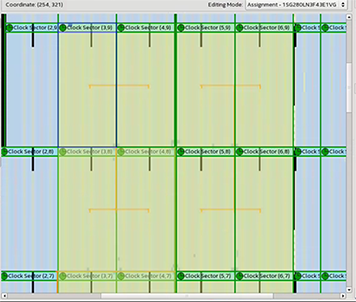
- On the Chip Planner Tasks pane, click Report Clock Details. The Chip Planner highlights the clock pin location, routing, and sector boundaries. Click elements under the Clock Details Report to display general and fan-out details for the element.
- To visualize the clock sector boundaries, click the Layers Settings tab and enable Clock Sector Region. The green lines indicate the boundaries of each sector.
Figure 63. Clock Network in Chip Planner
Figure 64. Clock Sector Boundary Layer in Chip Planner

