Follow these steps to get started with your Intel® Cyclone® 10 LP FPGA kit, and prepare your development environment.
- Verify basic board operation
- Download and install the Intel® Quartus® Prime Software Suite, Lite Edition
- Install the JTAG download cable driver
- Establish communication with the Intel® Nios® II processor
- Download the Intel® Cyclone® 10 LP FPGA kit reference designs and documentation
- Run the board test system application
Step 1: Verify Board Operation
-
Make sure DIP switch S1-4 (BYPASS) is in the default “OFF” position as shown in figure 1. This enables a JTAG connection to the board via USB. The other 3 switches are general user inputs and can be in any state.
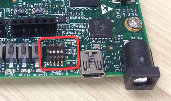
Figure 1 -
Plug the black USB Type A connector into your PC, and the Mini-B connector into the board.
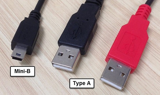
Figure 2 - Once powered the blue power LED, and yellow configuration LED's will light, while the four user LED's will flash in sequence. This indicates that the FPGA has been successfully programed from the external flash device with the Golden System Reference Design.
What is the Golden System Reference Design?
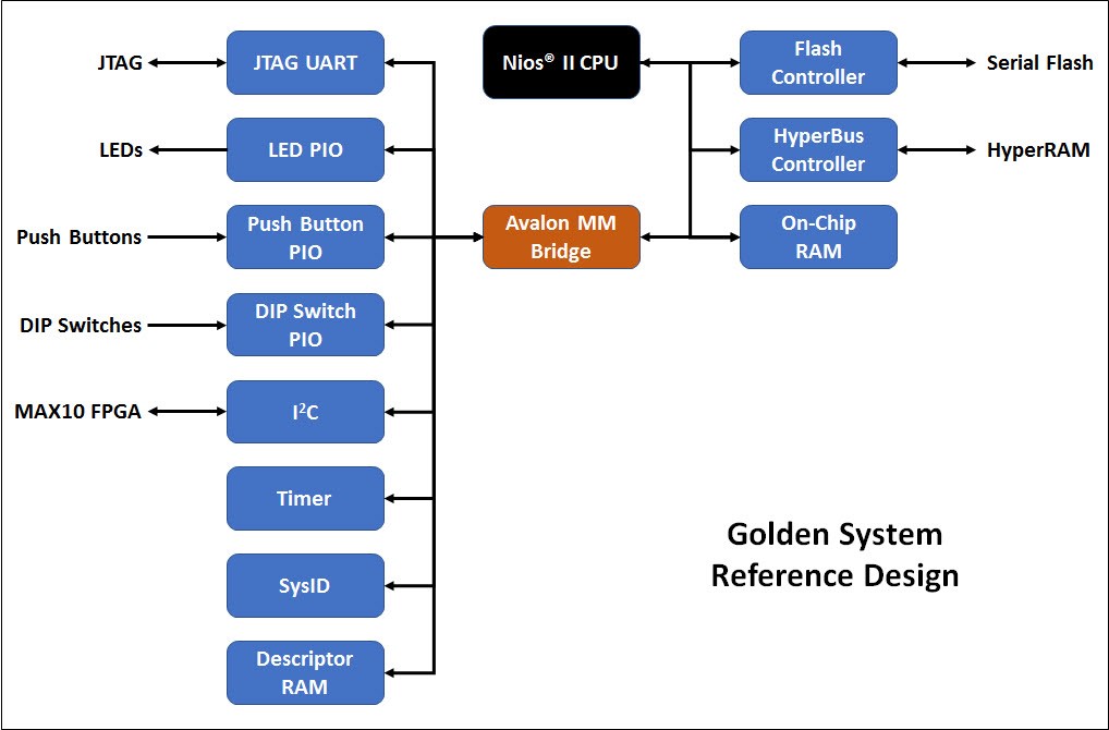
The Golden System Reference Design (GSRD) is the FPGA image that ships from the factory programmed into the on-board flash device, and which the FPGA loads immediately when power is applied. The block diagram below illustrates what is included in the GSRD. The source files for this design are included in the Kit Design Files available from the Intel® Cyclone® 10 LP Kit Downloads page.
Step 2: Download and Install the Intel® Quartus® Prime Software
The FPGA design software used here is ideal for beginners as it’s free to download and no license file is required. Click here to download the software.
Note: The installation files are large (several gigabytes) and can take a long time to download and install. To minimize download time and disk space required, we recommend you download only those items necessary. When prompted which files to download, uncheck “Select All” and select only Quartus Prime and Cyclone 10 device support only.
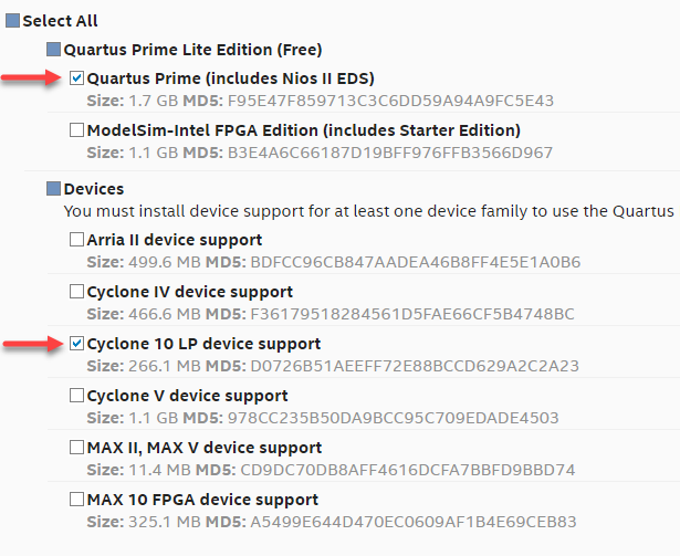
You will be prompted to log in you your myAltera account. If you don’t have an account yet, you can create one quickly and the download will begin. After the download is complete, an installer will launch automatically.
Why is the Intel® Quartus® Prime Software download so big?
The Intel® Quartus® software download contains several state-of-the-art tools needed to create a custom chip design, such as a simulator, synthesis tool, place and route engine, timing analyzer, and device programmer, to name a few. Nearly all those functions are built into the design software itself. The download also includes the embedded software design suite for the Nios® II processor, and one or more FPGA family databases - in our case the Intel® Cyclone® 10 FPGA database.
Step 3: Install the JTAG Cable Driver
The evaluation board design includes an integrated USB-Blaster II JTAG download cable for FPGA programming. However, before the host computer and board can communicate fully, you must install the driver on the host computer.
Installing the USB Download Cable Driver on Windows PCs:
To install the drivers for Windows PCs, you must have system administration (Administrator) privileges to install the USB-Blaster II download cable driver. With the evaluation kit connected to your PC via the USB cable, perform the following steps:
- Locate USB Download Cable driver in
\<Intel® Quartus® Prime system directory>\drivers\usb-blaster-ii.
If the driver is not in your directory, download the driver fromwww.altera.com/support/software/drivers. - Open the Device Manager on your PC. In the Other Devices tab, select and right click USB-Blaster. Then, click Update Driver Software.
- Click Browse. Browse to
\<Intel® Quartus® Prime system directory>\drivers\usb-blaster-iiand click Next. The Windows security warning is displayed. - Click Install to begin installing the driver.
- Click Finish when the driver is installed.
- Restart your system.
Installing the USB Download Cable Driver on Linux PCs:
Click here for instructions to install the USB-Blaster II driver for Linux
Step 4: Communicate with the Intel® Nios® II Processor
The Intel® Cyclone® 10 LP FPGA evaluation kit is pre-loaded with an Intel® Nios® II processor as part of the Golden System Reference Design (GSRD).
- Apply power to the evaluation kit, the blue power and yellow configuration LEDs will be lit while the green LEDs flash in sequence.
- Open the Windows Start menu, click All Programs > Intel FPGA > Nios II Command Shell.
- Launch the Intel® Nios® II processor terminal by typing: nios2-terminal
- The command shell prompt will return with the following results:
- nios2-terminal : connected to hardware target using JTAG UART on cable
- nios2-terminal : "Intel Cyclone 10 LP FPGA evaluation kit [USB-1]", device 1, instance 0
- nios2-terminal : (Use the IDE stop button or ctrl-c to terminate)
- Hello world !
- Press CTRL-C to exit the terminal.
- You have now successfully verified communication with the Intel® Nios® II processor.
Step 5: Download the Intel® Cyclone® 10 LP FPGA Evaluation Board Collateral
To download the Intel® Cyclone® 10 LP FPGA evaluation board package, perform the
following steps:
- Open a web browser and navigate to the Intel® Cyclone® 10 LP FPGA evaluation kit page here.
- Scroll to the bottom of the page and click on the Kit Collateral link.
- Unzip the kit collateral .zip file to your PC's local hard drive.
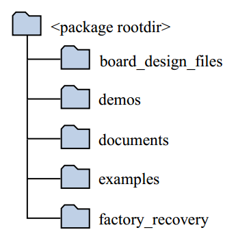
- The package creates the directory structure shown in the figure below.
| File Directory Name | Description of Directory Contents. |
|---|---|
| board_design_files | Contains schematics, layout, assembly and bill of material board design files. Use these files as a starting point for a new prototype board design. |
| demos | Contains demonstration applications when available. |
| documents | Contains the evaluation kit documentation. |
| examples | Contains the sample design files for the evaluation kit. |
| factory_recovery | Contains the original data programmed onto the board before shipment. Use this data to restore the board with its original factory contents. |
Step 6: Run the Board Test System (BTS) Application
The board test system application lets you to verify operation of most of the components on your board via an easy-to-use graphical user interface. It lets you modify clock operation, measure power usage, test memory, interact with the GPIO, and reconfigure the FPGA.
- Locate the board test system folder \<package rootdir>\examples\board_test_system.
-
Launch the
BoardTestSystem.exefrom the BTS folder and the screen shown in Figure 1 appears. At the base of the screen you will see a green indicator confirming that the board is connected and communicating with your PC. Hover your mouse over the photo to identify the various components on the board.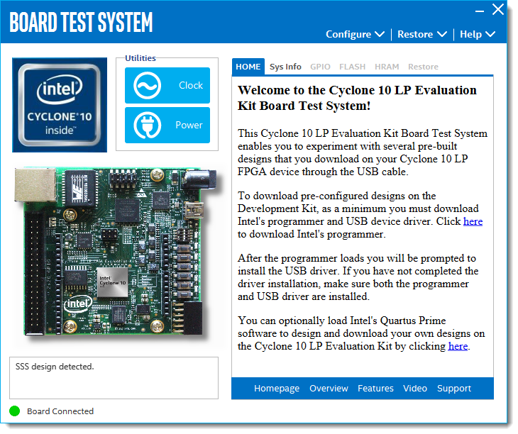
-
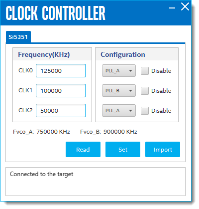
Click the Clock icon in the Utilities section to expose a window that lets you read or change the clock frequencies. For now, we won’t make any changes, so close the window.
-
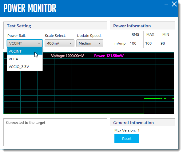
Click the Power icon in the Utilities section to measure device power consumption. You can select any of the three power rails to monitor from the Power Rail button. Close the window when you are ready to move on.
-
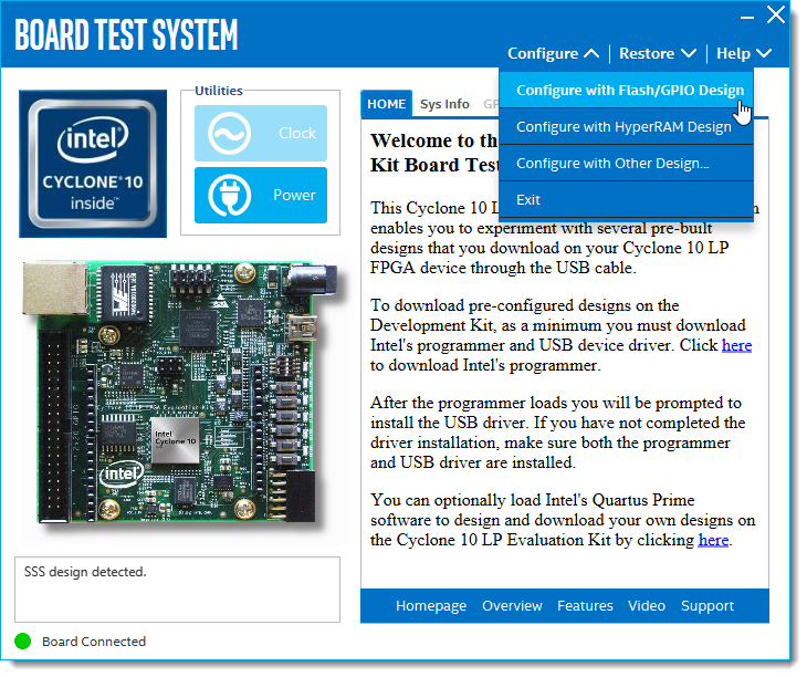
Reconfigure the FPGA with a new design that lets us interact with the Flash memory and GPIO. Click the Configure pull-down and select Configure with Flash/GPIO Design.
-
Click the Configure button to reconfigure the FPGA via the USB download cable.

-
The BTS GUI now displays tabs for interacting with the GPIO, and configuration flash memory.
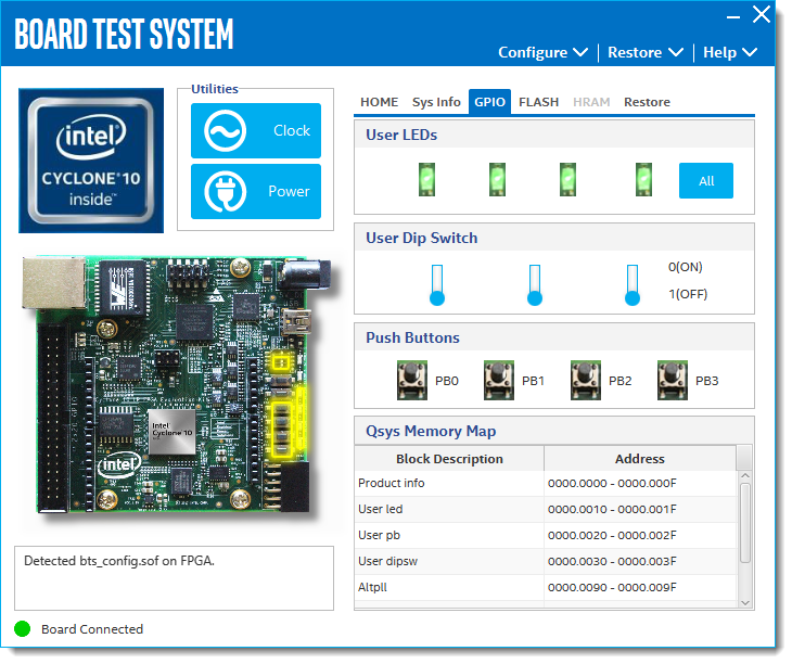
With the GPIO tab selected you can:
- Turn the user LEDs on and off by clicking the respective buttons
- Change the state of DIP switches 0 through 2 and watch the DIP switch indicators change. Be sure not to change the state of DIP switch 3 (JTAG Enable)
- Depress push buttons PB0 through PB3 and watch the button images change. Please do not press the CONF or RESET buttons which are the two closest to the DIP switches.
- View the memory map of the peripherals in the FPGA design
-
Select the Flash tab to see the contents, and memory map of the configuration flash.
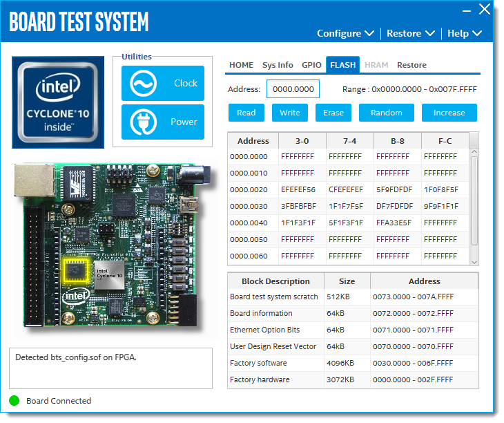
With this interface you can read, write and erase flash memory contents, but only within the Board Test System scratch address range (0073.0000 – 007A.FFFF).
-
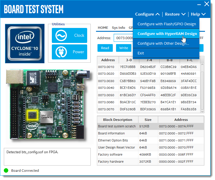
Let’s reconfigure the FPGA with a new design that lets us interact with the HyperRAM memory device. Click the Configure pull-down and select Configure with HyperRAM Design.
-
Click the Configure button to reconfigure the FPGA via the USB download cable.
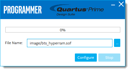
-
The BTS GUI now displays tabs for interacting with the HyperRAM memory.
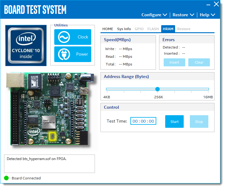
With the HyperRAM tab selected you can:
- Measure HyperRAM memory Read/Write speed
- Inject memory errors and observe error detection
- Select the memory range to use for testing (4KB to 16MB)
- For help using the BTS, click Help.
- When you are finished experimenting, close the BTS application.